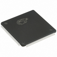
CY7C375I-125AC Cypress Semiconductor Corp, CY7C375I-125AC Datasheet - Page 6

CY7C375I-125AC
Manufacturer Part Number
CY7C375I-125AC
Description
IC CPLD 128 MACROCELL 160LQFP
Manufacturer
Cypress Semiconductor Corp
Series
Ultralogic™r
Specifications of CY7C375I-125AC
Memory Type
CMOS
Programmable Type
In-System Reprogrammable™ (ISR™) CMOS
Delay Time Tpd(1) Max
10.0ns
Voltage Supply - Internal
4.75 V ~ 5.25 V
Number Of Logic Elements/blocks
8
Number Of Macrocells
128
Number Of I /o
128
Operating Temperature
0°C ~ 70°C
Mounting Type
Surface Mount
Package / Case
160-LQFP
Voltage
5V
Family Name
FLASH370i
# Macrocells
128
Number Of Usable Gates
3200
Frequency (max)
158.3MHz
Propagation Delay Time
10ns
Number Of Logic Blocks/elements
8
# I/os (max)
128
Operating Supply Voltage (typ)
5V
In System Programmable
Yes
Operating Supply Voltage (min)
4.75V
Operating Supply Voltage (max)
5.25V
Operating Temp Range
0C to 70C
Operating Temperature Classification
Commercial
Mounting
Surface Mount
Pin Count
160
Package Type
TQFP
Lead Free Status / RoHS Status
Contains lead / RoHS non-compliant
Features
-
Number Of Logic Elements/cells
-
Lead Free Status / RoHS Status
Not Compliant, Contains lead / RoHS non-compliant
Other names
428-1472
Available stocks
Company
Part Number
Manufacturer
Quantity
Price
Company:
Part Number:
CY7C375I-125AC
Manufacturer:
CYPRESS
Quantity:
150
Company:
Part Number:
CY7C375I-125AC
Manufacturer:
Cypress Semiconductor Corp
Quantity:
10 000
Document #: 38-03029 Rev. *A
Maximum Ratings
(Above which the useful life may be impaired. For user guide-
lines, not tested.)
Storage Temperature ................................. –65°C to +150°C
Ambient Temperature with
Power Applied............................................. –55°C to +125°C
Supply Voltage to Ground Potential ............... –0.5V to +7.0V
DC Voltage Applied to Outputs
in High-Z State ............................................... –0.5V to +7.0V
DC Input Voltage............................................ –0.5V to +7.0V
DC Program Voltage .....................................................12.5V
Electrical Characteristics
Capacitance
V
V
V
V
V
I
I
I
I
I
I
I
I
C
C
Notes:
Parameter
10. Measured with 16-bit counter programmed into each logic block.
11. C
IX
OZ
OS
CC
BHL
BHH
BHLO
BHHO
2. T
3. See the last page of this specification for Group A subgroup testing information.
4. If V
5. I
6. When the I/O is three-stated, the bus-hold circuit can weakly pull the I/O to a maximum of 4.0V if no leakage current is allowed. This voltage is lowered significantly by
7. These are absolute values with respect to device ground. All overshoots due to system or tester noise are included.
8. Not more than one output should be tested at a time. Duration of the short circuit should not exceed 1 second. V
9. Tested initially and after any design or process changes that may affect these parameters.
OH
OHZ
OL
IH
IL
I/O
CLK
a small leakage current. Note that all I/Os are three-stated during ISR programming. Refer to the application note “Understanding Bus Hold” for additional information.
problems caused by tester ground degradation.
OH
A
[11]
I/O
Parameter
is the “instant on” case temperature.
CCIO
= –2 mA, I
for dedicated inputs, and for I/O pins with JTAG functionality is 12 pF,and for the ISR
is not specified, the device can be operating in either 3.3V or 5V I/O mode; V
Output HIGH Voltage
Output HIGH Voltage with Output
Disabled
Output LOW Voltage
Input HIGH Voltage
Input LOW Voltage
Input Load Current
Output Leakage Current
Output Short Circuit Current
Power Supply Current
Input Bus Hold LOW Sustaining Current V
Input Bus Hold HIGH Sustaining Current V
Input Bus Hold LOW Overdrive Current V
Input Bus Hold HIGH Overdrive Current V
OL
[9]
= 2 mA for SDO.
[9]
Input/Output Capacitance
Clock Signal Capacitance
Description
Description
Over the Operating Range
[10]
[8, 9]
V
V
V
Guaranteed Input Logical HIGH voltage for all
inputs
Guaranteed Input Logical LOW voltage for all
inputs
V
V
V
V
V
f = 1 MHz, V
CC
CC
CC
I
CC
CC
CC
CC
CC
CC
CC
CC
V
V
= Internal GND, V
IN
IN
= Max., V
= Max. I
= Min. I
= Min. I
= Max., V
= Max., V
= Max., I
= Min., V
= Min., V
= Max.
= Max.
[7]
[7]
= 5.0V at f=1 MHz
= 5.0V at f = 1 MHz
Test Conditions
[3, 4]
I
I
I
OH
OH
OH
OH
OL
OL
IN
O
OUT
IL
IH
O
OUT
= GND, V
= GND or V
Output Current into Outputs ........................................ 16 mA
Static Discharge Voltage........................................... > 2001V
(per MIL-STD-883, Method 3015)
Latch-up Current..................................................... > 200 mA
Operating Range
= 16 mA (Com’l/Ind)
= 12 mA (Mil)
Commercial
Industrial
Military
= –3.2 mA (Com’l/Ind)
= –2.0 mA (Mil)
= 0 µA (Com’l/Ind)
= –50 µA (Com’l/Ind)
= 0.8V
Test Conditions
= 2.0V
= 3.3V, Output Disabled
= 0 mA,
= 0.5V
Range
CC
I
=V
= V
EN
[2]
CCINT
CC
pin is 15 pF Max.
CC
O
= V
.
–55°C to +125°C 5V ± 0.5V
−40°C to +85°C
CC
Temperature
0°C to +70°C
, Output Disabled –50
Ambient
[5, 6]
Com’l/Ind.
Com’l “L” –66
Military
[5]
[5, 6]
[5]
Min.
[6]
OUT
5
= 0.5V has been chosen to avoid test
V
5V ± 0.25V 5V ± 0.25V or
5V ± 0.5V
CC
Min.
–0.5
+75
–10
–30
–75
2.4
2.0
0
V
Max.
CCINT
12
8
CY7C375i
Typ.
–70
125
125
75
5V ± 0.5V or
3.3V ± 0.3V
3.3V ± 0.3V
Page 6 of 17
Max. Unit
–125
–160 mA
+500 µA
–500
V
+10
+50
200
125
250
4.0
3.6
0.5
7.0
0.8
CCIO
Unit
pF
pF
mA
mA
mA
µA
µA
µA
µA
µA
µA
V
V
V
V
V
V
V
V


