XC2C128-7TQG144I Xilinx Inc, XC2C128-7TQG144I Datasheet
XC2C128-7TQG144I
Specifications of XC2C128-7TQG144I
Available stocks


Related parts for XC2C128-7TQG144I


XC2C128-7TQG144I Summary of contents
Page 1
... Xilinx, Inc. All rights reserved. All Xilinx trademarks, registered trademarks, patents, and disclaimers are as listed at http://www.xilinx.com/legal.htm. All other trademarks and registered trademarks are the property of their respective owners. All specifications are subject to change without notice. DS093 (v3.2) March 8, 2007 Product Specification 0 XC2C128 CoolRunner-II CPLD Product Specification 0 0 Description The CoolRunner-II 128-macrocell device is designed for both high performance and low power applications ...
Page 2
... LVTTL input buffer and Push-Pull output buffer. The LVCMOS standard is used in 3.3V, 2.5V, 1.8V applications. Both HSTL and SSTL make use compliance. CoolRunner-II CPLDs are also 1.5V I/O com- patible with the use of Schmitt-trigger inputs. Table 1). This Table 1: I/O Standards for XC2C128 IOSTANDARD Attribute LVTTL LVCMOS33 LVCMOS25 LVCMOS18 ...
Page 3
... CC CCIO V = 1.9V 3.6V CC CCIO MHz MHz MHz MHz MHz 3.9V IN CCIO 3.9V IN CCIO www.xilinx.com XC2C128 CoolRunner-II CPLD Value Units –0.5 to 2.0 V –0.5 to 4.0 V –0.5 to 4.0 V –0.5 to 4.0 V –0.5 to 4.0 V –0.5 to 4.0 V –65 to +150 °C + 150 °C Min Max Units 1.7 1 ...
Page 4
... XC2C128 CoolRunner-II CPLD LVCMOS and LVTTL 3.3V DC Voltage Specifications Symbol Parameter V Input source voltage CCIO V High level input voltage IH V Low level input voltage IL V High level output voltage OH V Low level output voltage OL LVCMOS 2.5V DC Voltage Specifications Symbol Parameter V Input source voltage ...
Page 5
... REF Test Conditions –8 mA CCIO mA CCIO , also peak to peak ac noise on V CCIO REF of receiving devices. REF Test Conditions V www.xilinx.com XC2C128 CoolRunner-II CPLD Min. Max. 0.4 = 1.4V 0.2 Min. Max. 1.4 3 CCIO CCIO 0 0 CCIO CCIO Min. Typ. Max. 2.3 2 ...
Page 6
... XC2C128 CoolRunner-II CPLD Symbol Parameter V High level output voltage OH V Low level output voltage OL Notes should track the variations in V REF transmitting device must track Test Conditions I = – CCIO mA 1.7V OL CCIO , also peak to peak ac noise on V CCIO REF of receiving devices. ...
Page 7
... OR array (one counter per function block). SYSTEM2 the maximum external frequency using one p-term while F EXT1 SU1 CO 4. Typical configuration current during DS093 (v3.2) March 8, 2007 Product Specification Parameter mA. CONFIG www.xilinx.com XC2C128 CoolRunner-II CPLD -6 -7 Min. Max. Min. Max. - 5.7 - 7.0 - 6.0 - 7.5 3 ...
Page 8
... XC2C128 CoolRunner-II CPLD Internal Timing Parameters Symbol Parameter Buffer Delays T Input buffer delay IN T Direct data register input delay DIN T Global Clock buffer delay GCK T Global set/reset buffer delay GSR T Global 3-state buffer delay GTS T Output buffer delay OUT T Output buffer enable/disable delay ...
Page 9
... GCK GSR - OUT , DIN GCK GSR - OUT , DIN GCK GSR - OUT Switching Test Conditions 8 16 DS093_02_050103 PD www.xilinx.com XC2C128 CoolRunner-II CPLD -6 -7 Max. Min. Max. 0.6 - 0.7 1.5 - 3.0 0.8 - 0.9 3.0 - 4.0 0.5 - 0.6 1.2 - 3.0 1.2 - 1.4 3.0 - 4.0 0 ...
Page 10
... The I/V curve illustrates the nominal amount of current that an I/O can source/sink at different voltage levels 1. Pin Descriptions 11 Function Macro- Block cell VQ100 CP132 TQ144 1(GTS1 1(GTS0 3.3V 2.5V 1.5V 1.0 1.5 2.0 VO (Output Volts) Figure 4: Typical I/V Curves for XC2C128 Pin Descriptions (Continued) Function I/O Block Bank 2(GCK0 2(GCK1 2(CDRST 2(GCK2 www.xilinx.com Iol 2.5 3.0 3 ...
Page 11
... A6 130 129 www.xilinx.com XC2C128 CoolRunner-II CPLD Macro- cell VQ100 CP132 TQ144 1 65 G13 G12 F14 F13 F12 E13 100 7 70 E12 101 D14 102 12 72 D13 103 13 73 D12 104 14 74 C14 105 15 76 B13 110 16 - A13 111 1 64 H12 ...
Page 12
... XC2C128 CoolRunner-II CPLD Pin Descriptions (Continued) Function Macro- Block cell VQ100 CP132 TQ144 Pin Descriptions (Continued) I/O Function Bank Block C12 112 2 8 B12 113 2 8 A12 115 2 8 C11 116 2 8 B11 117 2 8 A11 118 2 8 C10 119 A10 ...
Page 13
... R XC2C128 JTAG, Power/Ground, No Connect Pins and Total User I/O Pin Type TCK TDI TDO TMS V (JTAG supply voltage) CCAUX Power internal ( Power Bank 1 I CCIO1 Power Bank 2 I CCIO2 Ground No connects Total user I/O (including dual function pins) Notes: 1. Pin compatible with all larger and smaller densities except where I/O banking is used. ...
Page 14
... XC2C128 CoolRunner-II CPLD Pin/Ball Part Number Spacing XC2C128-7CP132I 0.5mm XC2C128-7TQ144I 0.5mm XC2C128-7VQG100I 0.5mm XC2C128-7CPG132I 0.5mm XC2C128-7TQG144I 0.5mm Notes Commercial (T = 0° +70° C Industrial (T A Standard Example: XC2C128 -6 TQ Device Speed Grade Package Type Number of Pins Temperature Range Device Part Marking Device Type ...
Page 15
... GND I/O (2) I/O (2) I/O (4) GND DS093 (v3.2) March 8, 2007 Product Specification VQ100 12 Top View Figure 6: VQ100 Very Thin Quad Flat Pack www.xilinx.com XC2C128 CoolRunner-II CPLD GND 75 I/O 74 I/O 73 I/O 72 I/O 71 I/O 70 GND 69 I I/O I I/O I GND 61 I/O 60 I/O 59 I/O 58 I/O ...
Page 16
... XC2C128 CoolRunner-II CPLD P VCC I/O(5) I/O GND I/O(2) I I/O(4) I I/O( I/O GND I/O(2) K I/O I/O VCCIO1 J H I/O I/O I/O G I/O I/O I/O I/O I/O I/O F I/O I/O I I/O I/O VAUX C I/O I/O(1) I/O(1) VCCIO2 B I/O I/O(1) GND I/O(1) VCC I/O(3) ...
Page 17
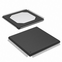
... AND ARE NOT WARRANTED FOR USE IN APPLICATIONS THAT POSE A RISK OF PHYSICAL HARM OR LOSS OF LIFE. USE OF PRODUCTS IN SUCH APPLICATIONS IS FULLY AT THE RISK OF CUSTOMER SUBJECT TO APPLICABLE LAWS AND REGULATIONS. DS093 (v3.2) March 8, 2007 Product Specification TQ144 Top View Figure 8: TQ144 Thin Quad Flat Pack www.xilinx.com XC2C128 CoolRunner-II CPLD GND 108 NC 107 NC 106 I/O 105 ...
Page 18
... XC2C128 CoolRunner-II CPLD Additional Information Additional information is available for the following CoolRunner-II topics: • XAPP784: Bulletproof CPLD Design Practices • XAPP375: Timing Model • XAPP376: Logic Engine • XAPP378: Advanced Features • XAPP382: I/O Characteristics • XAPP389: Powering CoolRunner-II • XAPP399: Assigning VREF Pins Revision History The following table shows the revision history for this document ...