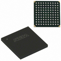
EPM570F100C4N Altera, EPM570F100C4N Datasheet - Page 54

EPM570F100C4N
Manufacturer Part Number
EPM570F100C4N
Description
IC MAX II CPLD 570 LE 100-FBGA
Manufacturer
Altera
Series
MAX® IIr
Specifications of EPM570F100C4N
Programmable Type
In System Programmable
Delay Time Tpd(1) Max
5.4ns
Voltage Supply - Internal
2.5V, 3.3V
Number Of Logic Elements/blocks
570
Number Of Macrocells
440
Number Of I /o
76
Operating Temperature
0°C ~ 85°C
Mounting Type
Surface Mount
Package / Case
100-FBGA
Voltage
2.5V, 3.3V
Memory Type
FLASH
Number Of Logic Elements/cells
570
Family Name
MAX II
# Macrocells
440
Frequency (max)
2.3148GHz
Propagation Delay Time
7ns
Number Of Logic Blocks/elements
57
# I/os (max)
76
Operating Supply Voltage (typ)
2.5/3.3V
In System Programmable
Yes
Operating Supply Voltage (min)
2.375V
Operating Supply Voltage (max)
3.6V
Operating Temp Range
0C to 85C
Operating Temperature Classification
Commercial
Mounting
Surface Mount
Pin Count
100
Package Type
FBGA
No. Of I/o's
76
Propagation Delay
7ns
Global Clock Setup Time
1.5ns
Frequency
247.5MHz
Supply Voltage Range
2.375V To 2.625V, 3V To 3.6V
Operating Temperature Range
0°C To +85°C
Rohs Compliant
Yes
Lead Free Status / RoHS Status
Lead free / RoHS Compliant
Features
-
Lead Free Status / Rohs Status
Compliant
Other names
544-1716
Available stocks
Company
Part Number
Manufacturer
Quantity
Price
Company:
Part Number:
EPM570F100C4N
Manufacturer:
ALTERA
Quantity:
12 388
Company:
Part Number:
EPM570F100C4N
Manufacturer:
ALTERA
Quantity:
325
Part Number:
EPM570F100C4N
Manufacturer:
ALTERA/阿尔特拉
Quantity:
20 000
4–4
Figure 4–2. Transistor-Level Diagram of MAX II Device I/O Buffers
Figure 4–3. ESD Protection During Positive Voltage Zap
MAX II Device Handbook
n+
The CMOS output drivers in the I/O pins intrinsically provide electrostatic discharge
(ESD) protection. There are two cases to consider for ESD voltage strikes: positive
voltage zap and negative voltage zap.
A positive ESD voltage zap occurs when a positive voltage is present on an I/O pin
due to an ESD charge event. This can cause the N+ (Drain)/ P-Substrate junction of
the N-channel drain to break down and the N+ (Drain)/P-Substrate/N+ (Source)
intrinsic bipolar transistor turn on to discharge ESD current from I/O pin to GND.
The dashed line (see
positive ESD zap.
IOE Signal
p - well
I/O
n+
GND
VPAD
Figure
Source
Drain
Drain
Source
PMOS
NMOS
4–3) shows the ESD current discharge path during a
Larger of VCCIO or VPAD
p+
IOE Signal or the
Gate
Gate
Chapter 4: Hot Socketing and Power-On Reset in MAX II Devices
n - well
Hot Socketing Feature Implementation in MAX II Devices
P-Substrate
VCCIO
p+
p - substrate
N+
N+
VCCIO or VPAD
The Larger of
D
S
n+
GND
I/O
G
© October 2008 Altera Corporation
Ensures 3.3-V
Tolerance and
Hot-Socket
Protection


