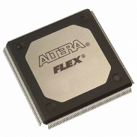
EPM9560ARI240-10 Altera, EPM9560ARI240-10 Datasheet - Page 20

EPM9560ARI240-10
Manufacturer Part Number
EPM9560ARI240-10
Description
IC MAX 9000 CPLD 560 240-RQFP
Manufacturer
Altera
Series
MAX® 9000r
Datasheet
1.EPM9320LC84-15.pdf
(46 pages)
Specifications of EPM9560ARI240-10
Programmable Type
In System Programmable
Delay Time Tpd(1) Max
10.0ns
Voltage Supply - Internal
4.5 V ~ 5.5 V
Number Of Logic Elements/blocks
35
Number Of Macrocells
560
Number Of Gates
12000
Number Of I /o
191
Operating Temperature
-40°C ~ 85°C
Mounting Type
Surface Mount
Package / Case
240-RQFP
Voltage
3.3V/5V
Memory Type
EEPROM
Number Of Logic Elements/cells
35
Family Name
MAX 9000
# Macrocells
560
Number Of Usable Gates
12000
Frequency (max)
144.9MHz
Propagation Delay Time
10ns
Number Of Logic Blocks/elements
35
# I/os (max)
191
Operating Supply Voltage (typ)
5V
In System Programmable
Yes
Operating Supply Voltage (min)
4.5V
Operating Supply Voltage (max)
5.5V
Operating Temp Range
-40C to 85C
Operating Temperature Classification
Industrial
Mounting
Surface Mount
Pin Count
240
Package Type
RQFP
Lead Free Status / RoHS Status
Contains lead / RoHS non-compliant
Features
-
Lead Free Status / Rohs Status
Not Compliant
Other names
544-2365
Available stocks
Company
Part Number
Manufacturer
Quantity
Price
Company:
Part Number:
EPM9560ARI240-10
Manufacturer:
ALTERA
Quantity:
6
Part Number:
EPM9560ARI240-10
Manufacturer:
ALTERA/阿尔特拉
Quantity:
20 000
MAX 9000 Programmable Logic Device Family Data Sheet
20
Programming Sequence
During in-system programming, instructions, addresses, and data are
shifted into the MAX 9000 device through the TDI input pin. Data is
shifted out through the TDO output pin and compared against the
expected data.
Programming a pattern into the device requires the following six ISP
stages. A stand-alone verification of a programmed pattern involves only
stages 1, 2, 5, and 6.
1.
2.
3.
4.
5.
6.
Programming Times
The time required to implement each of the six programming stages can
be broken into the following two elements:
Enter ISP. The enter ISP stage ensures that the I/O pins transition
smoothly from user mode to ISP mode. The enter ISP stage requires
1 ms.
Check ID. Before any program or verify process, the silicon ID is
checked. The time required to read this silicon ID is relatively small
compared to the overall programming time.
Bulk Erase. Erasing the device in-system involves shifting in the
instructions to erase the device and applying one erase pulse of
100 ms.
Program. Programming the device in-system involves shifting in the
address and data and then applying the programming pulse to
program the EEPROM cells. This process is repeated for each
EEPROM address.
Verify. Verifying an Altera device in-system involves shifting in
addresses, applying the read pulse to verify the EEPROM cells, and
shifting out the data for comparison. This process is repeated for
each EEPROM address.
Exit ISP. An exit ISP stage ensures that the I/O pins transition
smoothly from ISP mode to user mode. The exit ISP stage requires
1 ms.
A pulse time to erase, program, or read the EEPROM cells.
A shifting time based on the test clock (TCK) frequency and the
number of TCK cycles to shift instructions, address, and data into the
device.
Altera Corporation


