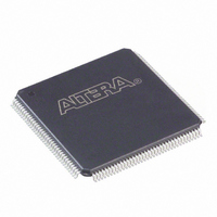
EPM570T144I5N Altera, EPM570T144I5N Datasheet - Page 60

EPM570T144I5N
Manufacturer Part Number
EPM570T144I5N
Description
IC MAX II CPLD 570 LE 144-TQFP
Manufacturer
Altera
Series
MAX® IIr
Specifications of EPM570T144I5N
Programmable Type
In System Programmable
Delay Time Tpd(1) Max
5.4ns
Voltage Supply - Internal
2.5V, 3.3V
Number Of Logic Elements/blocks
570
Number Of Macrocells
440
Number Of I /o
116
Operating Temperature
-40°C ~ 100°C
Mounting Type
Surface Mount
Package / Case
144-TQFP, 144-VQFP
Voltage
2.5V, 3.3V
Memory Type
FLASH
Number Of Logic Elements/cells
570
Lead Free Status / RoHS Status
Lead free / RoHS Compliant
Features
-
Other names
544-2283
Available stocks
Company
Part Number
Manufacturer
Quantity
Price
Company:
Part Number:
EPM570T144I5N
Manufacturer:
ALTERA52
Quantity:
980
Part Number:
EPM570T144I5N
Manufacturer:
ALTERA/阿尔特拉
Quantity:
20 000
5–2
Recommended Operating Conditions
Table 5–2. MAX II Device Recommended Operating Conditions
MAX II Device Handbook
V
V
V
V
T
Notes to
(1) MAX II device in-system programming and/or user flash memory (UFM) programming via JTAG or logic array is not guaranteed outside the
(2) Minimum DC input is –0.5 V. During transitions, the inputs may undershoot to –2.0 V for input currents less than 100 mA and periods shorter
(3) During transitions, the inputs may overshoot to the voltages shown in the following table based upon input duty cycle. The DC case is equivalent
(4) All pins, including clock, I/O, and JTAG pins, may be driven before V
(5) For the extended temperature range of 100 to 125º C, MAX II UFM programming (erase/write) is only supported via the JTAG interface. UFM
J
CCINT
CCIO
I
O
Symbol
recommended operating conditions (for example, if brown-out occurs in the system during a potential write/program sequence to the UFM,
users are recommended to read back UFM contents and verify against the intended write data).
than 20 ns.
to 100% duty cycle. For more information about 5.0-V tolerance, refer to the
MAX II Device Handbook.
V
4.0 V
4.1
4.2
4.3
4.4
4.5
programming via the logic array interface is not guaranteed in this range.
(1)
IN
(1)
Table
Max. Duty Cycle
100% (DC)
17%
90%
50%
30%
10%
3.3-V supply voltage for internal logic and
ISP
2.5-V supply voltage for internal logic and
ISP
1.8-V supply voltage for internal logic and
ISP
Supply voltage for I/O buffers, 3.3-V
operation
Supply voltage for I/O buffers, 2.5-V
operation
Supply voltage for I/O buffers, 1.8-V
operation
Supply voltage for I/O buffers, 1.5-V
operation
Input voltage
Output voltage
Operating junction temperature
5–2:
Table 5–2
Parameter
shows the MAX II device family recommended operating conditions.
MAX II devices
MAX II devices
MAX IIG and MAX IIZ
devices
Commercial range
Industrial range
Extended range
CC INT
and V
(2), (3),
Conditions
Using MAX II Devices in Multi-Voltage Systems
C CIO
—
—
—
—
—
are powered.
(4)
(5)
Chapter 5: DC and Switching Characteristics
Minimum
2.375
2.375
1.425
3.00
1.71
3.00
1.71
–0.5
–40
–40
0
0
© August 2009 Altera Corporation
Maximum
Operating Conditions
2.625
2.625
1.575
3.60
1.89
3.60
1.89
V
100
125
4.0
85
C CIO
chapter in the
Unit
°C
°C
°C
V
V
V
V
V
V
V
V
V


