EPM240GM100C5N Altera, EPM240GM100C5N Datasheet - Page 55
EPM240GM100C5N
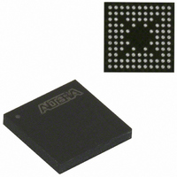
Manufacturer Part Number
EPM240GM100C5N
Description
IC MAX II CPLD 240 LE 100-MBGA
Manufacturer
Altera
Series
MAX® IIr
Datasheets
1.EPM240GT100C5N.pdf
(6 pages)
2.EPM240GT100C5N.pdf
(88 pages)
3.EPM240GM100C5N.pdf
(10 pages)
Specifications of EPM240GM100C5N
Programmable Type
In System Programmable
Delay Time Tpd(1) Max
4.7ns
Voltage Supply - Internal
1.71 V ~ 1.89 V
Number Of Logic Elements/blocks
240
Number Of Macrocells
192
Number Of I /o
80
Operating Temperature
0°C ~ 85°C
Mounting Type
Surface Mount
Package / Case
100-MBGA
Voltage
1.8V
Memory Type
FLASH
Number Of Logic Elements/cells
240
Family Name
MAX II
# Macrocells
192
Frequency (max)
1.8797GHz
Propagation Delay Time
7.5ns
Number Of Logic Blocks/elements
24
# I/os (max)
80
Operating Supply Voltage (typ)
1.8V
In System Programmable
Yes
Operating Supply Voltage (min)
1.71V
Operating Supply Voltage (max)
1.89V
Operating Temp Range
0C to 85C
Operating Temperature Classification
Commercial
Mounting
Surface Mount
Pin Count
100
Package Type
MBGA
Lead Free Status / RoHS Status
Lead free / RoHS Compliant
Features
-
Lead Free Status / Rohs Status
Compliant
Other names
544-1726
Available stocks
Company
Part Number
Manufacturer
Quantity
Price
Company:

Part Number:
EPM240GM100C5N
Manufacturer:
CYPESS
Quantity:
1
Company:
Part Number:
EPM240GM100C5N
Manufacturer:
ALTERA10
Quantity:
1 287
Part Number:
EPM240GM100C5N
Manufacturer:
ALTERA/阿尔特拉
Quantity:
20 000


Chapter 4: Hot Socketing and Power-On Reset in MAX II Devices
Power-On Reset Circuitry
Figure 4–4. ESD Protection During Negative Voltage Zap
Power-On Reset Circuitry
© October 2008 Altera Corporation
When the I/O pin receives a negative ESD zap at the pin that is less than –0.7 V (0.7 V
is the voltage drop across a diode), the intrinsic
P-Substrate/N+ drain diode is forward biased. Therefore, the discharge ESD current
path is from GND to the I/O pin, as shown in
MAX II devices have POR circuits to monitor V
power-up. The POR circuit monitors these voltages, triggering download from the
non-volatile configuration flash memory (CFM) block to the SRAM logic, maintaining
tri-state of the I/O pins (with weak pull-up resistors enabled) before and during this
process. When the MAX II device enters user mode, the POR circuit releases the I/O
pins to user functionality. The POR circuit of the MAX II (except MAX IIZ) device
continues to monitor the V
POR circuit of the MAX IIZ device does not monitor the V
device enters into user mode. More details are provided in the following sub-sections.
I/O
GND
Source
Drain
Drain
Source
CCINT
PMOS
NMOS
voltage level to detect a brown-out condition. The
Gate
Gate
P-Substrate
Figure
CCINT
N+
N+
and V
D
S
4–4.
GND
I/O
G
CCIO
CCINT
voltage levels during
voltage level after the
MAX II Device Handbook
4–5
Related parts for EPM240GM100C5N
Image
Part Number
Description
Manufacturer
Datasheet
Request
R

Part Number:
Description:
CYCLONE II STARTER KIT EP2C20N
Manufacturer:
Altera
Datasheet:


Part Number:
Description:
CPLD, EP610 Family, ECMOS Process, 300 Gates, 16 Macro Cells, 16 Reg., 16 User I/Os, 5V Supply, 35 Speed Grade, 24DIP
Manufacturer:
Altera Corporation
Datasheet:
Part Number:
Description:
CPLD, EP610 Family, ECMOS Process, 300 Gates, 16 Macro Cells, 16 Reg., 16 User I/Os, 5V Supply, 15 Speed Grade, 24DIP
Manufacturer:
Altera Corporation
Datasheet:
Part Number:
Description:
Manufacturer:
Altera Corporation
Datasheet:
Part Number:
Description:
CPLD, EP610 Family, ECMOS Process, 300 Gates, 16 Macro Cells, 16 Reg., 16 User I/Os, 5V Supply, 30 Speed Grade, 24DIP
Manufacturer:
Altera Corporation
Datasheet:
Part Number:
Description:
High-performance, low-power erasable programmable logic devices with 8 macrocells, 10ns
Manufacturer:
Altera Corporation
Datasheet:
Part Number:
Description:
High-performance, low-power erasable programmable logic devices with 8 macrocells, 7ns
Manufacturer:
Altera Corporation
Datasheet:
Part Number:
Description:
Classic EPLD
Manufacturer:
Altera Corporation
Datasheet:
Part Number:
Description:
High-performance, low-power erasable programmable logic devices with 8 macrocells, 10ns
Manufacturer:
Altera Corporation
Datasheet:
Part Number:
Description:
Manufacturer:
Altera Corporation
Datasheet:
Part Number:
Description:
Manufacturer:
Altera Corporation
Datasheet:
Part Number:
Description:
Manufacturer:
Altera Corporation
Datasheet:
Part Number:
Description:
CPLD, EP610 Family, ECMOS Process, 300 Gates, 16 Macro Cells, 16 Reg., 16 User I/Os, 5V Supply, 25 Speed Grade, 24DIP
Manufacturer:
Altera Corporation
Datasheet: