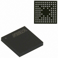
EPM240GM100C5N Altera, EPM240GM100C5N Datasheet - Page 19

EPM240GM100C5N
Manufacturer Part Number
EPM240GM100C5N
Description
IC MAX II CPLD 240 LE 100-MBGA
Manufacturer
Altera
Series
MAX® IIr
Datasheets
1.EPM240GT100C5N.pdf
(6 pages)
2.EPM240GT100C5N.pdf
(88 pages)
3.EPM240GM100C5N.pdf
(10 pages)
Specifications of EPM240GM100C5N
Programmable Type
In System Programmable
Delay Time Tpd(1) Max
4.7ns
Voltage Supply - Internal
1.71 V ~ 1.89 V
Number Of Logic Elements/blocks
240
Number Of Macrocells
192
Number Of I /o
80
Operating Temperature
0°C ~ 85°C
Mounting Type
Surface Mount
Package / Case
100-MBGA
Voltage
1.8V
Memory Type
FLASH
Number Of Logic Elements/cells
240
Family Name
MAX II
# Macrocells
192
Frequency (max)
1.8797GHz
Propagation Delay Time
7.5ns
Number Of Logic Blocks/elements
24
# I/os (max)
80
Operating Supply Voltage (typ)
1.8V
In System Programmable
Yes
Operating Supply Voltage (min)
1.71V
Operating Supply Voltage (max)
1.89V
Operating Temp Range
0C to 85C
Operating Temperature Classification
Commercial
Mounting
Surface Mount
Pin Count
100
Package Type
MBGA
Lead Free Status / RoHS Status
Lead free / RoHS Compliant
Features
-
Lead Free Status / Rohs Status
Compliant
Other names
544-1726
Available stocks
Company
Part Number
Manufacturer
Quantity
Price
Company:
Part Number:
EPM240GM100C5N
Manufacturer:
CYPESS
Quantity:
1
Company:
Part Number:
EPM240GM100C5N
Manufacturer:
ALTERA10
Quantity:
1 287
Part Number:
EPM240GM100C5N
Manufacturer:
ALTERA/阿尔特拉
Quantity:
20 000
Chapter 2: MAX II Architecture
Logic Elements
Figure 2–9. Carry-Select Chain
© October 2008 Altera Corporation
LAB Carry-In
A1
B1
A2
B2
A3
B3
A4
B4
A6
B6
A7
B7
A8
B8
A9
B9
A10
B10
A5
B5
The speed advantage of the carry-select chain is in the parallel precomputation of
carry chains. Since the LAB carry-in selects the precomputed carry chain, not every LE
is in the critical path. Only the propagation delays between LAB carry-in generation
(LE 5 and LE 10) are now part of the critical path. This feature allows the MAX II
architecture to implement high-speed counters, adders, multipliers, parity functions,
and comparators of arbitrary width.
Figure 2–9
portion of the LUT generates the sum of two bits using the input signals and the
appropriate carry-in bit; the sum is routed to the output of the LE. The register can be
bypassed for simple adders or used for accumulator functions. Another portion of the
LUT generates carry-out bits. An LAB-wide carry-in bit selects which chain is used for
the addition of given inputs. The carry-in signal for each chain, carry-in0 or
carry-in1, selects the carry-out to carry forward to the carry-in signal of the next-
higher-order bit. The final carry-out signal is routed to an LE, where it is fed to local,
row, or column interconnects.
LAB Carry-Out
0
0
LE0
LE1
LE2
LE3
LE4
LE5
LE6
LE7
LE8
LE9
1
1
Sum1
Sum2
Sum3
Sum4
Sum5
Sum6
Sum7
Sum8
Sum9
Sum10
shows the carry-select circuitry in an LAB for a 10-bit full adder. One
To top of adjacent LAB
LAB Carry-In
Carry-In0
Carry-In1
data1
data2
Carry-Out0
LUT
LUT
LUT
LUT
Carry-Out1
Sum
MAX II Device Handbook
2–11


