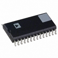
AD1859JR Analog Devices Inc, AD1859JR Datasheet - Page 15

AD1859JR
Manufacturer Part Number
AD1859JR
Description
IC DAC STEREO SNGL-SUP 5V 28SOIC
Manufacturer
Analog Devices Inc
Datasheet
1.AD1859JR.pdf
(16 pages)
Specifications of AD1859JR
Rohs Status
RoHS non-compliant
Number Of Bits
18
Data Interface
DSP, I²S, Serial, SPI™
Number Of Converters
2
Voltage Supply Source
Analog and Digital
Power Dissipation (max)
330mW
Operating Temperature
-40°C ~ 105°C
Mounting Type
Surface Mount
Package / Case
28-SOIC (7.5mm Width)
Settling Time
-
Available stocks
Company
Part Number
Manufacturer
Quantity
Price
Company:
Part Number:
AD1859JR
Manufacturer:
AD
Quantity:
4 530
Company:
Part Number:
AD1859JRS
Manufacturer:
AD
Quantity:
5 510
Part Number:
AD1859JRS
Manufacturer:
ADI/亚德诺
Quantity:
20 000
Part Number:
AD1859JRSZ
Manufacturer:
ADI/亚德诺
Quantity:
20 000
Part Number:
AD1859JRZ
Manufacturer:
ADI/亚德诺
Quantity:
20 000
REV. A
Figure 30. 1 kHz Tone at –90 dBFS (16K-Point FFT) Includ-
ing Time Domain Plot Bandlimited to 22 kHz
Application Circuits
Figure 32 illustrates a 600 ohm line driver using the Analog
Devices SSM2017 and SSM2142 components. Figure 33
illustrates a “Numerically Controlled Oscillator” (NCO) that
can be implemented in programmable logic or a system ASIC to
provide the synchronous bit and left/right clocks from 27 MHz
for MPEG audio decoders. Note that the bit clock and left/right
clock outputs are highly jittered, but this jitter should be
14
13
12
10
21
20
19
11
16
15
9
8
2
7
100n
C11
BCLK
LRCLK
SDATA
IDPM1
IDPM0
18/16
CLATCH
CDATA
CCLK
PD/RST
DEEMP
MUTE
XTALI/MCLK
XTALO
–100
–110
–120
–130
–140
–90
–10
–20
–30
–40
–50
–60
–70
–80
0
17
DGND
18
+5V
DV
0
AD1859-JR
DD
DD
2k
+5V
23
AV
AGND
6
DD
CC
CMOUT
4k
OUTL
EMPL
OUTR
EMPR
FGND
FILT
100n
C12
6k
4
3
25
26
1
28
27
100n
V
C9
8k
FREQUENCY – Hz
REF
1Vrms
1Vrms
100
10
0%
90
10k 12k
2.25V
+
–
4µ7
C10
R1, 2k49
R2, 2k49
14k
100n
100n
C8
C1
3
1
8
2
3
1
8
2
16k
Figure 32. 600 Ohm Balanced Line Driver
RG
RG
–IN
RG
RG
–IN
+IN
+IN
+15V
–15V
–15V
+15V
1
2
1
2
7
7
18k
V+
V+
V–
V–
4
4
REF
REF
100n
OUT
OUT
100n
5
5
C6
C7
20k
U2
SSM2017P
U3
SSM2017P
6
6
22k
–15–
5Vrms
5Vrms
perfectly acceptable. MPEG audio decoders are insensitive to
this clock jitter (using these signals to clock audio data from their
output serial port, and perhaps to decrement their audio/video
synchronization timer), while the AD1859 will reject the left/right
clock jitter by virtue of its on-chip digital phase locked loop.
Contact Analog Devices Computer Products Division Customer
Support at (617) 461-3881 or cpd_support@analog.com for more
information on this NCO circuit.
4
3
4
3
Figure 31. Digital Filter Signal Transfer Function to
3.5
V
V
GND
GND
IN
SSM2142P
IN
SSM2142P
–100
–110
–120
–130
–140
–150
–160
–15V
–15V
+15V
5
+15V
5
–10
–30
–40
–50
–60
–70
–80
–90
6
6
–20
+V
–V
+V
–V
U4
U5
+SENSE
+SENSE
–SENSE
–SENSE
0
0.0
F
+OUT
+OUT
–OUT
–OUT
S
100n
100n
C5
C3
8
7
2
1
8
7
2
1
C4
100n
C2
100n
0.5
1.0
1
2
3
4
5
J1 P1
1.5
1
2
3
4
5
F
S
2.0
MAX OUTPUT EACH
CHANNEL
10Vrms (166.7mV V = +22dBm)
INTO 600
2.5
P2 J2
1
2
3
4
5
AD1859
1
2
3
4
5
3.0
600
600
3.5
R3
R4


