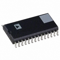
AD1859JR Analog Devices Inc, AD1859JR Datasheet - Page 10

AD1859JR
Manufacturer Part Number
AD1859JR
Description
IC DAC STEREO SNGL-SUP 5V 28SOIC
Manufacturer
Analog Devices Inc
Datasheet
1.AD1859JR.pdf
(16 pages)
Specifications of AD1859JR
Rohs Status
RoHS non-compliant
Number Of Bits
18
Data Interface
DSP, I²S, Serial, SPI™
Number Of Converters
2
Voltage Supply Source
Analog and Digital
Power Dissipation (max)
330mW
Operating Temperature
-40°C ~ 105°C
Mounting Type
Surface Mount
Package / Case
28-SOIC (7.5mm Width)
Settling Time
-
Available stocks
Company
Part Number
Manufacturer
Quantity
Price
Company:
Part Number:
AD1859JR
Manufacturer:
AD
Quantity:
4 530
Company:
Part Number:
AD1859JRS
Manufacturer:
AD
Quantity:
5 510
Part Number:
AD1859JRS
Manufacturer:
ADI/亚德诺
Quantity:
20 000
Part Number:
AD1859JRSZ
Manufacturer:
ADI/亚德诺
Quantity:
20 000
Part Number:
AD1859JRZ
Manufacturer:
ADI/亚德诺
Quantity:
20 000
AD1859
The serial control port is byte oriented. The data is MSB first,
and is unsigned. There is a control register for the left channel
and a control register for the right channel, as distinguished by
the MSB (DATA7). The bits are assigned as shown in Figure 8.
The left channel control register and the right channel control reg-
ister have identical power up and reset default settings. DATA6,
the Mute control bit, reset default state is LO, which is the nor-
mal (nonmuted) setting. DATA5:0, the Atten5 through Atten0
control bits, have a reset default value of 00 0000, which is an
attenuation of 0.0 dB (i.e., full scale, no attenuation). The intent
with these reset defaults is to enable AD1859 applications with-
out requiring the use of the serial control port. For those users
that do not use the serial control port, it is still possible to mute
the AD1859 output by using the external MUTE (Pin 7) signal.
It is recommended that the output be muted for approximately
1000 input sample periods during power-up or following any
radical sample rate change (>5%) to allow the digital phase
locked loop to settle.
Note that the serial control port timing is asynchronous to the
serial data input port timing. Changes made to the attenuator
level will be updated on the next edge of the LRCLK after the
CLATCH write pulse. The AD1859 has been designed to re-
solve the potential for metastability between the LRCLK edge
and the CLATCH write pulse rising edge. The attenuator set-
ting is guaranteed to be valid even if the LRCLK edge and the
CLATCH rising edge occur essentially simultaneously.
On-Chip Oscillator and Master Clock
The asynchronous master clock of the AD1859 can be supplied
by either an external clock source applied to XTALI/MCLK or
by connecting a crystal across the XTALI/MCLK and XTALO
pins, and using the on-chip oscillator. If a crystal is used, it
should be fundamental-mode and parallel-tuned. Figure 9
shows example connections.
The range of audio sample rates (as determined from the
LRCLK input) supported by the AD1859 is a function of the
master clock rate (i.e., the crystal frequency or external clock
source frequency) applied. The highest sample rate supported
can be computed as follows:
CLATCH
CDATA
CCLK
Right Channel = HI
Left Channel = LO
LEFT/RIGHT
DATA7
MSB
MSB
D7
D6
Mute = HI
Normal = LO
DATA6
Mute
D5
Figure 8. Serial Control Bit Definitions
Figure 7. Serial Control Port Timing
D4
DATA5
Atten5
D3
DATA4
Atten4
D2
–10–
The lowest sample rate supported can be computed as follows:
Figure 10 illustrates these relations. As can be seen in Figure 10,
a 27 MHz MCLK or crystal frequency supports audio sample
rates from approximately 28 kHz to 52 kHz.
Mute and Attenuation
The AD1859 offers two methods of muting the analog output.
By asserting the MUTE (Pin 7) signal HI, both the left channel
and the right channel are muted. As an alternative, the user can
assert the mute bit in the serial control registers HI for indi-
vidual mute of either the left channel or the right channel. The
D1
DATA3
Atten3
Figure 10. MCLK Frequency vs. L/ R Clock Frequency
00 0000 = 0.0dB
00 0001 = –1.0dB
00 0010 = –2.0dB
00 0011 = –3.0dB
00 0100 = –4.0dB
00 0101 = –5.0dB
00 0110 = –6.0dB
00 0111 = –7.0dB
00 1000 = –8.0dB
11 1101 = –61.0dB
11 1110 = –62.0dB
11 1111 = –63.0dB
20-64pF
Lowest Sample Rate = Master Clock Frequency
Highest Sample Rate = Master Clock Frequency
27MHz CRYSTAL CONNECTION
LSB
Figure 9. Crystal and Oscillator Connections
D0
76
68
60
52
44
36
28
20
XTALI/MCLK
*
*
*
DATA2
Atten2
18
AD1859
27MHz
20
XTALO
DATA1
Atten1
22
XTAL/MCLK FREQUENCY – MHz
20-64pF
24
MSB
26
DATA0
Atten0
D7
27MHz OSCILLATOR CONNECTION
LSB
L/R SAMPLE RATE
XTALI/MCLK
28
(MCLK/512)
D6
27MHz
HIGHEST
L/R SAMPLE RATE
30
AD1859
(MCLK/1024)
D5
LOWEST
32
XTALO
NC
34
1024
512
REV. A
36


