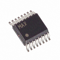
MAX5155ACEE+ Maxim Integrated Products, MAX5155ACEE+ Datasheet - Page 14

MAX5155ACEE+
Manufacturer Part Number
MAX5155ACEE+
Description
IC DAC 12BIT DUAL LP SER 16-QSOP
Manufacturer
Maxim Integrated Products
Datasheet
1.MAX5154BCEE.pdf
(16 pages)
Specifications of MAX5155ACEE+
Settling Time
15µs
Number Of Bits
12
Data Interface
Serial
Number Of Converters
2
Voltage Supply Source
Single Supply
Power Dissipation (max)
667mW
Operating Temperature
0°C ~ 70°C
Mounting Type
Surface Mount
Package / Case
16-QSOP
Resolution
12 bit
Interface Type
Serial (3-Wire, SPI, QSPI, Microwire)
Supply Voltage (max)
3.6 V
Supply Voltage (min)
2.7 V
Maximum Operating Temperature
+ 70 C
Mounting Style
SMD/SMT
Minimum Operating Temperature
0 C
Lead Free Status / RoHS Status
Lead free / RoHS Compliant
The MAX5154/MAX5155 can be configured for a bipo-
lar output, as shown in Figure 11. The output voltage is
given by the equation (OS_ = AGND):
where NB represents the numeric value of the DAC’s
binary input code. Table 3 shows digital codes and the
corresponding output voltage for Figure 11’s circuit.
In applications where the reference has an AC signal
component, the MAX5154/MAX5155 have multiplying
capabilities within the reference input voltage range
specifications. Figure 12 shows a technique for apply-
Low-Power, Dual, 12-Bit Voltage-Output DACs
with Serial Interface
14
Table 3. Bipolar Code Table
Note: ( ) are for the sub bit.
Figure 11. Bipolar Output Circuit
MSB
1 1 1 1 1 1 1 1 1 1 1 1 ( 0 )
1 0 0 0 0 0 0 0 0 0 0 1 ( 0 )
1 0 0 0 0 0 0 0 0 0 0 0 ( 0 )
0 1 1 1 1 1 1 1 1 1 1 1 ( 0 )
0 0 0 0 0 0 0 0 0 0 0 1 ( 0 )
0 0 0 0 0 0 0 0 0 0 0 0 ( 0 )
REF_
______________________________________________________________________________________
DAC CONTENTS
DAC _
MAX5154
MAX5155
V
OUT
+5V/+3V
DGND
V
= V
DD
LSB
REF
R
R
AGND
[((2 x NB) / 4096) - 1]
Using an AC Reference
OUT_
OS_
-V
10k
10k
ANALOG OUTPUT
REF
10k
+V
+V
-V
-V
Bipolar Output
REF
REF
REF
2048
2048
REF
0V
V+
V-
2047
2048
10k
2048
2048
2047
2048
1
1
- V
REF
V
OUT
ing a sinusoidal input to REF_, where the AC signal is
offset before being applied to the reference input.
The total harmonic distortion plus noise (THD+N) is typ-
ically less than -78dB at full scale with a 1Vp-p input
swing at 5kHz. The typical -3dB frequency is 300kHz
for both devices, as shown in the Typical Operating
Characteristics.
Figure 13 shows the MAX5154/MAX5155 in a digital
calibration application. With a bright light value applied
to the photodiode (on), the DAC is digitally ramped until
Figure 13. Digital Calibration
Figure 12. AC Reference Input Circuit
REFERENCE
500mVp-p
+5V/
P
+3V
INPUT
AC
DIN
26k
REF_
AGND
DAC _
10k
MAX5154
MAX5155
Harmonic Distortion and Noise
+5V/+3V
+5V/+3V
V
DD
AGND
DAC_
Digital Calibration and
REF
MAX495
DGND
Threshold Selection
R
R
MAX5154
MAX5155
OUT_
OS_
V
DD
DGND
V+
R
R
PHOTODIODE
PULLDOWN
R
V+
V-
OS_
OUT_
V
OUT


