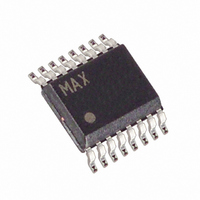
MAX5155ACEE+ Maxim Integrated Products, MAX5155ACEE+ Datasheet - Page 11

MAX5155ACEE+
Manufacturer Part Number
MAX5155ACEE+
Description
IC DAC 12BIT DUAL LP SER 16-QSOP
Manufacturer
Maxim Integrated Products
Datasheet
1.MAX5154BCEE.pdf
(16 pages)
Specifications of MAX5155ACEE+
Settling Time
15µs
Number Of Bits
12
Data Interface
Serial
Number Of Converters
2
Voltage Supply Source
Single Supply
Power Dissipation (max)
667mW
Operating Temperature
0°C ~ 70°C
Mounting Type
Surface Mount
Package / Case
16-QSOP
Resolution
12 bit
Interface Type
Serial (3-Wire, SPI, QSPI, Microwire)
Supply Voltage (max)
3.6 V
Supply Voltage (min)
2.7 V
Maximum Operating Temperature
+ 70 C
Mounting Style
SMD/SMT
Minimum Operating Temperature
0 C
Lead Free Status / RoHS Status
Lead free / RoHS Compliant
Figure 3. Connections for SPI/QSPI
Figure 4. Serial-Data Format
Figure 5. Serial-Interface Timing Diagram
MSB...................................................................................LSB
Address Bits
1 Address/2 Control Bits
Low-Power, Dual, 12-Bit Voltage-Output DACs
A0
MAX5154
MAX5155
SCLK
DIN
CS
Control Bits
SCLK
______________________________________________________________________________________
16 Bits of Serial Data
C1, C0
DIN
CS
A0
1
C1
MSB...DataBits...LSB
D11.......................D0
C0 D11 D10
12 Data Bits
CPOL = 0, CPHA = 0
MOSI
SCK
I/O
SPI/QSPI
PORT
D9
+5V
SS
D8
SUB
BIT
S0
D7
0
8
D6
The MAX5154/MAX5155’s digital inputs are double
buffered, which allows any of the following: loading the
input register(s) without updating the DAC register(s),
updating the DAC register(s) from the input register(s),
or updating the input and DAC registers concurrently.
The address and control bits allow the DACs to act
independently.
Send the 16-bit data as one 16-bit word (QSPI) or two
8-bit packets (SPI, Microwire), with CS low during this
period. The address and control bits determine which
register will be updated, and the state of the registers
when exiting shutdown. The 3-bit address/control deter-
mines the following:
• registers to be updated
• clock edge on which data is to be clocked out via
• state of the user-programmable logic output
• configuration of the device after shutdown.
The general timing diagram of Figure 5 illustrates how
data is acquired. Driving CS low enables the device to
receive data. Otherwise, the interface control circuitry is
disabled. With CS low, data at DIN is clocked into the
register on the rising edge of SCLK. As CS goes high,
data is latched into the input and/or DAC registers
depending on the address and control bits. The maxi-
mum clock frequency guaranteed for proper operation
is 10MHz. Figure 6 depicts a more detailed timing dia-
gram of the serial interface.
9
D5
the serial-data output (DOUT)
with Serial Interface
D4
D3
D2
D1
D0
S0
16
COMMAND
EXECUTED
11


