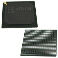
LFE3-150EA-8FN1156C Lattice, LFE3-150EA-8FN1156C Datasheet - Page 10

LFE3-150EA-8FN1156C
Manufacturer Part Number
LFE3-150EA-8FN1156C
Description
IC FPGA 149K LUTS 586I/O FN1156
Manufacturer
Lattice
Series
ECP3r
Datasheets
1.LFE3-150EA-7FN672C.pdf
(136 pages)
2.LFE3-35EA-8FN672I.pdf
(4 pages)
3.LFE3-35EA-8FN672I.pdf
(21 pages)
Specifications of LFE3-150EA-8FN1156C
Number Of Logic Elements/cells
149000
Number Of Labs/clbs
18625
Total Ram Bits
7014400
Number Of I /o
586
Number Of Gates
-
Voltage - Supply
1.14 V ~ 1.26 V
Mounting Type
Surface Mount
Operating Temperature
0°C ~ 85°C
Package / Case
1156-BBGA
Lead Free Status / Rohs Status
Lead free / RoHS Compliant
Available stocks
Company
Part Number
Manufacturer
Quantity
Price
Company:
Part Number:
LFE3-150EA-8FN1156C
Manufacturer:
Transcend
Quantity:
1 000
Part Number:
LFE3-150EA-8FN1156C
Manufacturer:
LATTICE
Quantity:
20 000
Company:
Part Number:
LFE3-150EA-8FN1156CTW
Manufacturer:
Lattice Semiconductor Corporation
Quantity:
10 000
Lattice Semiconductor
Figure 2-4. General Purpose PLL Diagram
Table 2-4 provides a description of the signals in the PLL blocks.
Table 2-4. PLL Blocks Signal Descriptions
Delay Locked Loops (DLL)
In addition to PLLs, the LatticeECP3 family of devices has two DLLs per device.
CLKI is the input frequency (generated either from the pin or routing) for the DLL. CLKI feeds into the output muxes
block to bypass the DLL, directly to the DELAY CHAIN block and (directly or through divider circuit) to the reference
input of the Phase Detector (PD) input mux. The reference signal for the PD can also be generated from the Delay
Chain signals. The feedback input to the PD is generated from the CLKFB pin or from a tapped signal from the
Delay chain.
The PD produces a binary number proportional to the phase and frequency difference between the reference and
feedback signals. Based on these inputs, the ALU determines the correct digital control codes to send to the delay
CLKI
CLKFB
RST
RSTK
WRDEL
CLKOS
CLKOP
CLKOK
CLKOK2
LOCK
FDA [3:0]
DRPAI[3:0]
DFPAI[3:0]
DRPAI[3:0]
DFPAI[3:0]
FDA[3:0]
WRDEL
CLKFB
RSTK
Signal
CLKI
RST
I/O
O
O
O
O
O
I
I
I
I
I
I
I
I
CLKFB
Divider
Divider
Clock input from external pin or routing
PLL feedback input from CLKOP, CLKOS, or from a user clock (pin or logic)
“1” to reset PLL counters, VCO, charge pumps and M-dividers
“1” to reset K-divider
DPA Fine Delay Adjust input
PLL output to clock tree (phase shifted/duty cycle changed)
PLL output to clock tree (no phase shift)
PLL output to clock tree through secondary clock divider
PLL output to clock tree (CLKOP divided by 3)
“1” indicates PLL LOCK to CLKI
Dynamic fine delay adjustment on CLKOS output
Dynamic coarse phase shift, rising edge setting
Dynamic coarse phase shift, falling edge setting
CLKI
PFD
Loop Filter
VCO/
2-7
Description
CLKOP
Divider
Detect
Lock
LatticeECP3 Family Data Sheet
Duty Cycle/
Duty Trim
Duty Trim
CLKOK
Phase/
Divider
3
Architecture
CLKOK2
CLKOS
CLKOP
CLKOK
LOCK


