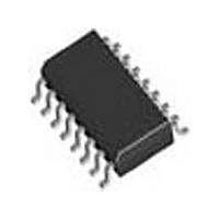
SI3018-F-FSR Silicon Laboratories Inc, SI3018-F-FSR Datasheet - Page 51

SI3018-F-FSR
Manufacturer Part Number
SI3018-F-FSR
Description
Modem Chip Chipset 16-Pin SOIC T/R
Manufacturer
Silicon Laboratories Inc
Datasheet
1.SI3018-F-FSR.pdf
(112 pages)
Specifications of SI3018-F-FSR
Package
16SOIC
Main Category
Chipset
Sub-category
Data/Voice
Typical Operating Supply Voltage
3.3 V
Power Supply Type
Digital
Typical Supply Current
8.5 mA
Minimum Operating Supply Voltage
3 V
Maximum Operating Supply Voltage
3.6 V
Data Rate
54.6875Kbps
Operating Supply Voltage (typ)
3.3V
Operating Supply Voltage (min)
3V
Operating Supply Voltage (max)
3.6V
Operating Temp Range
0C to 70C
Operating Temperature Classification
Commercial
Pin Count
16
Mounting
Surface Mount
Lead Free Status / Rohs Status
Compliant
Available stocks
Company
Part Number
Manufacturer
Quantity
Price
Company:
Part Number:
SI3018-F-FSR
Manufacturer:
SiliconL
Quantity:
52 026
Company:
Part Number:
SI3018-F-FSR
Manufacturer:
SILICON
Quantity:
57
Part Number:
SI3018-F-FSR
Manufacturer:
SILICONLABS/芯科
Quantity:
20 000
In this manner, multiple consecutive registers can be
read or written in one transmission sequence. By
correctly manipulating the MX and MR bits, a
transmission sequence can continue from the beginning
specified address until an invalid memory location is
reached. To end a transmission sequence, the host
processor must signal an end-of-message (EOM) by
placing the downstream MX and MR bits inactive for two
consecutive frames. The transmission also can be
stopped by the Si3050 by signaling an Abort. This is
signaled by placing the upstream MR bit inactive for at
least two consecutive cycles in response to the
downstream MX bit going active. An abort is signaled by
the Si3050 for the following reasons:
When the Si3050 aborts because of an invalid
command sequence, the state of the Si3050 does not
change. If a read or write to an invalid memory address
is attempted, all previous reads or writes in that
transmission sequence are valid up to the read or write
to the invalid memory address. If an EOM is detected
before a valid command sequence is communicated,
the Si3050 returns to the idle state and remains
unchanged.
A read or write to an invalid memory address is
attempted
An invalid command sequence is received
A data byte was not received for at least two
consecutive frames
A collision occurs on the Monitor data bytes while
the Si3050 is transmitting data
Rev. 1.31
The data presented to the Si3050 in the downstream
Monitor bits must be present for two consecutive frames
to be considered valid data. The Si3050 checks to
ensure it receives the same data in two consecutive
frames. If not, it does not acknowledge receipt of the
data byte and waits until it does receive two consecutive
identical data bytes before acknowledging to the
transmitter that it received the data. If the transmitter
attempts to signal transmission of a subsequent data
byte by placing the downstream MX bit in an inactive
state while the Si3050 is still waiting to receive a valid
data byte transmission of two consecutive identical data
bytes, the Si3050 signals an abort and ends the
transmission. Figure 43 shows a state diagram for the
Receiver Monitor channel for the Si3050. Figure 44 on
page 53 shows a state diagram for the Transmitter
Monitor channel for the Si3050.
Si3050 + Si3018/19
51


