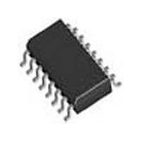
SI3018-F-FSR Silicon Laboratories Inc, SI3018-F-FSR Datasheet - Page 35

SI3018-F-FSR
Manufacturer Part Number
SI3018-F-FSR
Description
Modem Chip Chipset 16-Pin SOIC T/R
Manufacturer
Silicon Laboratories Inc
Datasheet
1.SI3018-F-FSR.pdf
(112 pages)
Specifications of SI3018-F-FSR
Package
16SOIC
Main Category
Chipset
Sub-category
Data/Voice
Typical Operating Supply Voltage
3.3 V
Power Supply Type
Digital
Typical Supply Current
8.5 mA
Minimum Operating Supply Voltage
3 V
Maximum Operating Supply Voltage
3.6 V
Data Rate
54.6875Kbps
Operating Supply Voltage (typ)
3.3V
Operating Supply Voltage (min)
3V
Operating Supply Voltage (max)
3.6V
Operating Temp Range
0C to 70C
Operating Temperature Classification
Commercial
Pin Count
16
Mounting
Surface Mount
Lead Free Status / Rohs Status
Compliant
Available stocks
Company
Part Number
Manufacturer
Quantity
Price
Company:
Part Number:
SI3018-F-FSR
Manufacturer:
SiliconL
Quantity:
52 026
Company:
Part Number:
SI3018-F-FSR
Manufacturer:
SILICON
Quantity:
57
Part Number:
SI3018-F-FSR
Manufacturer:
SILICONLABS/芯科
Quantity:
20 000
3. Assert the ONHM bit (Register 5, bit 3) to enable
4. Clear the ONHM bit after the caller ID data is
5.25.2. Type II Caller ID (Si3019 Line-Side Device
Type II Caller ID sends the CID data while the phone is
off-hook. This mode is often referred to as caller ID/
call waiting (CID/CW). To receive the CID data when
off-hook, use the following procedure (also see
Figure 24):
1. The Caller Alert Signal (CAS) tone is sent from the
2. The DAA must check if there is another parallel
caller ID data detection. The caller ID data is passed
across the RNG 1/2 pins and presented to the host
via the DTX pin.
received.
central office (CO) and is digitized along with the line
data. The host processor detects the presence of
this tone.
device on the same line, which is accomplished by
briefly going on-hook, measuring the line voltage,
and returning to an off-hook state.
a. Set the CALD bit (Register 17, bit 5) to disable
b. Set the RCALD bit (Register 25, bit 5) to disable
c. Set the FOH[1:0] bits (Register 31 bits 6:5) to 11
d. Clear the OH bit (Register 5, bit 0). This puts the
e. Read the LVS bits to determine the state of the
Only)
the calibration that automatically occurs when
going off-hook.
the resistor calibration that automatically occurs
when going off-hook
to reduce the time period for the off-hook counter
to 8 ms allowing compliance to the Type II CID
timing requirements.
DAA into an on-hook state. The RXM bit
(Register 15, bit 3) also can be set to mute the
receive path.
line. If the LVS bits read the typical on-hook line
voltage, then there are no parallel devices active
on the line, and CID data reception can be
continued. If the LVS bits read well below the
typical on-hook line voltage, then there are one or
more devices present and active on the same line
that are not compliant with Type II CID. Do not
continue CID data reception.
Rev. 1.31
3. The CO then responds with CID data after receiving
4. The muting of the upstream data path by the host
5. The CALD and the RCALD bits can be cleared to
Because of the nature of the low-power ADC, the data
presented on DTX can have up to a 10% dc offset. The
caller ID decoder must either use a high-pass or a
band-pass filter to accurately retrieve the caller ID data.
the CID data, the host processor unmutes the
upstream data output and continues with normal
operation.
processor mutes the handset in a telephone
application so the user cannot hear the
acknowledgement tone and CID data being sent.
re-enable the automatic calibrations when going
off-hook. The FOH[1:0] bits also can be programmed
to 01 to restore the default off-hook counter time.
f. Set the OH bit to return to an off-hook state.
Immediately after returning to an off-hook state,
the off-hook counter must be allowed to expire.
This allows the line voltage to settle before
transmitting or receiving data. After 8 ms normal
data transmission and reception can begin. If a
non-compliant parallel device is present, then a
reply tone is not sent by the host tone generator
and the CO does not send the CID data. If all
devices on the line are Type II CID compliant,
then the host must mute its upstream data output
to avoid the propagation of its reply tone and the
subsequent CID data. When muting its upstream
data output, the host processor should return an
acknowledgement (ACK) tone to the CO
requesting transmission of CID data.
Si3050 + Si3018/19
35


