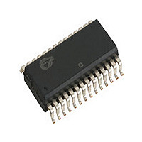
STK10C48-N25I Cypress Semiconductor Corp, STK10C48-N25I Datasheet - Page 9

STK10C48-N25I
Manufacturer Part Number
STK10C48-N25I
Description
Manufacturer
Cypress Semiconductor Corp
Type
NVSRAMr
Datasheet
1.STK10C48-N25I.pdf
(12 pages)
Specifications of STK10C48-N25I
Word Size
8b
Organization
2Kx8
Density
16Kb
Interface Type
Parallel
Access Time (max)
25ns
Operating Supply Voltage (typ)
5V
Package Type
SOIC
Operating Temperature Classification
Industrial
Operating Supply Voltage (max)
5.5V
Operating Supply Voltage (min)
4.5V
Operating Temp Range
-40C to 85C
Pin Count
28
Mounting
Surface Mount
Supply Current
90mA
Lead Free Status / Rohs Status
Not Compliant
March 2006
If the STK10C48 is in a
power-up
To help avoid this situation, a 10K Ohm resistor
should be connected either between W and system
V
HARDWARE PROTECT
The STK10C48 offers two levels of protection to
suppress inadvertent
signals (E, G, W and NE) remain in the
dition at the end of a
cycle will not be started. The
will be initiated only after a transition on any one of
these signals to the required state. In addition to
multi-trigger protection,
V
STORE
CC
CC
or between E and system V
is below 4.0V, protecting against inadvertent
100
s.
80
60
40
20
0
RECALL
Figure 2: I
50
, the
STORE
STORE
Cycle Time (ns)
SRAM
CC
STORE
100
WRITE
(max) Reads
cycle, a second
data will be corrupted.
cycles. If the control
s are inhibited when
STORE
150
CC
state at the end of
.
TTL
CMOS
200
(or
STORE
RECALL
STORE
con-
)
9
LOW AVERAGE ACTIVE POWER
The STK10C48 draws significantly less current
when it is cycled at times longer than 55ns. Figure 2
shows the relationship between I
time. Worst-case current consumption is shown for
both
perature range, V
enable). Figure 3 shows the same relationship for
WRITE
than 100%, only standby current is drawn when the
chip is disabled. The overall average current drawn
by the STK10C48 depends on the following items:
1)
chip enable; 3) the overall cycle rate for accesses;
4) the ratio of
temperature; 6) the V
CMOS
Document Control # ML0002 rev 0.2
CMOS
100
cycles. If the chip enable duty cycle is less
80
60
40
20
0
vs.
and
Figure 3: I
TTL
READ
TTL
CC
50
input levels; 2) the duty cycle of
= 5.5V, 100% duty cycle on chip
s to
input levels (commercial tem-
CC
Cycle Time (ns)
CC
level; and 7) I/O loading.
100
(max) Writes
WRITE
150
s; 5) the operating
CC
TTL
CMOS
and
STK10C48
200
READ
cycle


