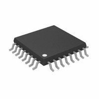
AD5764RCSUZ Analog Devices Inc, AD5764RCSUZ Datasheet - Page 25

AD5764RCSUZ
Manufacturer Part Number
AD5764RCSUZ
Description
IC DAC QUAD 16BIT VOUT 32-TQFP
Manufacturer
Analog Devices Inc
Datasheet
1.AD5764RBSUZ.pdf
(32 pages)
Specifications of AD5764RCSUZ
Data Interface
Serial
Design Resources
High Accuracy, Bipolar Voltage Output Digital-to-Analog Conversion Using AD5764 (CN0006)
Settling Time
8µs
Number Of Bits
16
Number Of Converters
4
Voltage Supply Source
Dual ±
Power Dissipation (max)
275mW
Operating Temperature
-40°C ~ 85°C
Mounting Type
Surface Mount
Package / Case
32-TQFP, 32-VQFP
Resolution (bits)
16bit
Sampling Rate
1.26MSPS
Input Channel Type
Serial
Supply Voltage Range - Digital
2.7V To 5.25V
Supply Current
3.55mA
Digital Ic Case Style
QFP
Lead Free Status / RoHS Status
Lead free / RoHS Compliant
Available stocks
Company
Part Number
Manufacturer
Quantity
Price
Company:
Part Number:
AD5764RCSUZ
Manufacturer:
Analog Devices Inc
Quantity:
10 000
Company:
Part Number:
AD5764RCSUZ-REEL7
Manufacturer:
Analog Devices Inc
Quantity:
10 000
DATA REGISTER
The data register is addressed by setting the three REG bits to 010. The DAC address bits select the DAC channel with which the data
transfer takes place (see Table 10). The data bits are positioned in DB15 to DB0, as shown in Table 13.
Table 13. Programming the Data Register
REG2
0
COARSE GAIN REGISTER
The coarse gain register is addressed by setting the three REG bits to 011. The DAC address bits select the DAC channel with which the
data transfer takes place (see Table 10). The coarse gain register is a 2-bit register that allows the user to select the output range of each
DAC, as shown in Table 15.
Table 14. Programming the Coarse Gain Register
Table 15. Output Range Selection
Output Range
±10 V (Default)
±10.2564 V
±10.5263 V
FINE GAIN REGISTER
The fine gain register is addressed by setting the three REG bits to 100. The DAC address bits select the DAC channel with which the data
transfer takes place (see Table 10). The AD5764R fine gain register is a 6-bit register that allows the user to adjust the gain of each DAC
channel by −32 LSBs to +31 LSBs in 1 LSB steps, as shown in Table 16 and Table 17. The adjustment is made to both the positive full-scale
points and the negative full-scale points simultaneously, with each point adjusted by one-half of one step. The fine gain register coding is
twos complement.
Table 16. Programming the Fine Gain Register
1
Table 17. Fine Gain Register Options
Gain Adjustment
+31 LSBs
+30 LSBs
No Adjustment (Default)
−31 LSBs
−32 LSBs
REG2
REG2
0
0
REG1
REG1
1
REG1
0
1
REG0
FG5
0
0
0
1
1
A2
REG0
1
REG0
0
DAC address
A1
A2
FG4
1
1
0
0
0
A0
DAC address
A2
CG1
0
0
1
Rev. B | Page 25 of 32
A1
DB15 to DB6
Don’t care
DAC address
FG3
1
1
0
0
0
A1
A0
A0
FG2
1
1
0
0
0
DB5
FG5
DB15 to DB2
Don’t care
DB4
FG4
FG1
1
1
0
0
0
DB3
FG3
CG0
0
1
0
16-bit DAC data
DB15 to DB0
DB2
FG2
DB1
CG1
FG0
1
0
0
1
0
DB1
AD5764R
FG1
DB0
CG0
DB0
FG0


