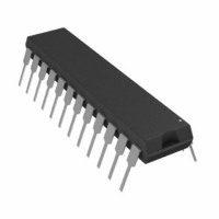
DAC8248FP Analog Devices Inc, DAC8248FP Datasheet - Page 14

DAC8248FP
Manufacturer Part Number
DAC8248FP
Description
IC DAC 12BIT DUAL BUFFERD 24-DIP
Manufacturer
Analog Devices Inc
Datasheet
1.DAC8248FPZ.pdf
(16 pages)
Specifications of DAC8248FP
Rohs Status
RoHS non-compliant
Settling Time
1µs
Number Of Bits
12
Data Interface
Parallel
Number Of Converters
2
Voltage Supply Source
Single Supply
Power Dissipation (max)
50µW
Operating Temperature
-40°C ~ 85°C
Mounting Type
Through Hole
Package / Case
24-DIP (0.300", 7.62mm)
Available stocks
Company
Part Number
Manufacturer
Quantity
Price
Part Number:
DAC8248FP
Manufacturer:
ADI/亚德诺
Quantity:
20 000
DAC8248
ground as shown in Figure 9. The output voltage will be be-
tween +5 V and +10 V depending on the digital input code.
The output expression is given by:
where V
VOLTAGE SWITCHING MODE
Figure 10 shows the DAC8248 in another single supply configu-
ration. The R-2R ladder is used in the voltage switching mode
and functions as a voltage divider. The output voltage (at the
V
must be buffered by an op amp. The R
are left open. The reference input voltage must be maintained
within +1.25 V of AGND, and V
this ensures that device accuracy is preserved.
The output voltage expression is given by:
where D = Decimal Equivalent of the Digital Input Word
REF
pin) exhibits a constant impedance R (typically 11 k ) and
D = Decimal Equivalent of the Digital Input Word
OS
= Offset Reference Voltage (+5 V in Figure 9)
V
OUT
V
OUT
= V
Figure 9. Single Supply Operation (Current Switching Mode)
= V
OS
REF
(D/4096)(V
DD
(D/4096)
between +12 V and +15 V;
FB
pins are not used and
OS
)
–14–
APPLICATIONS TIPS
GENERAL GROUND MANAGEMENT
Grounding techniques should be tailored to each individual sys-
tem. Ground loops should be avoided, and ground current paths
should be as short as possible and have a low impedance.
The DAC8248’s AGND and DGND pins should be tied to-
gether at the device socket to prevent digital transients from ap-
pearing at the analog output. This common point then becomes
the single ground point connection. AGND and DGND is then
brought out separately and tied to their respective power supply
grounds. Ground loops can be created if both grounds are tied
together at more than one location, i.e., tied together at the de-
vice and at the digital and analog power supplies.
PC board ground plane can be used for the single point ground
connection should the connections not be practical at the device
socket. If neither of these connections are practical or allowed,
then the device should be placed as close as possible to the sys-
tems single point ground connection. Back-to-back Schottky di-
odes should then be connected between AGND and DGND.
POWER SUPPLY DECOUPLING
Power supplies used with the DAC8248 should be well filtered
and regulated. Local supply decoupling consisting of a 1 F to
10 F tantalum capacitor in parallel with a 0.1 F ceramic is
highly recommended. The capacitors should be connected be-
tween the V
DD
and DGND pins and at the device socket.
REV. B


