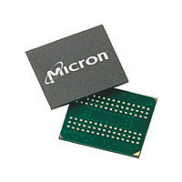
MT48V16M32L2B5-8 IT Micron Technology Inc, MT48V16M32L2B5-8 IT Datasheet

MT48V16M32L2B5-8 IT
Specifications of MT48V16M32L2B5-8 IT
Related parts for MT48V16M32L2B5-8 IT
MT48V16M32L2B5-8 IT Summary of contents
Page 1
... Temperature Commercial (0°C to +70°C) Industrial (-40°C to +85°C) PDF: 09005aef817f1b8c/Source: 09005aef818112f1 512Mb Mobile SDRAM_TwinDie_x32.fm - Rev. C 6/05 EN Products and specifications discussed herein are subject to change by Micron without notice. 512Mb : x32 TwinDie Mobile SDRAM Addendum Addendum Changes The standard 256Mb SDRAM Mobile x32 data sheets should be referenced for a complete description of SDRAM functionality and operating modes ...
Page 2
... A0-A12 select the row). The address bits registered coincident with the READ or WRITE command are used to select the starting column location for the burst access. The SDRAM provides for programmable READ or WRITE burst lengths locations, or the full page, with a burst terminate option. An auto precharge function may be enabled to provide a self-timed row precharge that is initiated at the end of the burst sequence ...
Page 3
... AUTO REFRESH command every 7.81µs will meet the refresh requirement and ensure that each row is refreshed. Alternatively, 8,192 AUTO REFRESH commands can be issued in a burst at the minimum cycle rate ( Figure 1: Functional Block Diagram PDF: 09005aef817f1b8c/Source: 09005aef818112f1 512Mb Mobile SDRAM_TwinDie_x32.fm - Rev. C 6/05 EN 512Mb : x32 TwinDie Mobile SDRAM Addendum t RC), once every 64ms. CS CLK ...
Page 4
... Ball Assignment Figure 2: 90-Ball FBGA Assignment PDF: 09005aef817f1b8c/Source: 09005aef818112f1 512Mb Mobile SDRAM_TwinDie_x32.fm - Rev. C 6/05 EN 512Mb : x32 TwinDie Mobile SDRAM Addendum DQ26 DQ24 DQ28 DQ27 DQ25 DQ29 DQ30 DQ31 DQM3 A12 J CLK CKE A9 K DQM1 DQ8 DQ10 DQ9 DQ12 DQ14 SS P DQ11 ...
Page 5
... DC Electrical Characteristics and Operating Conditions (LC version +3.3V ±0. Notes please refer to the 256Mb: x32 Mobile SDRAM data sheet for all notes. Parameter/Condition Supply Voltage Input High Voltage: Logic 1; All inputs Input Low Voltage: Logic 0; All inputs Input Leakage Current: Any input 0V ≤ V ≤ ...
Page 6
... OUT Table 6: I Specifications and Conditions (LC version +3.3V ±0.3V Notes 11, 13; please refer to the 256Mb: x32 Mobile SDRAM data sheet for all notes. Parameter/Condition Operating Current: Active Mode; Burst = 2; READ or WRITE (MIN) Standby Current: Power-Down Mode; All banks idle; CKE = LOW Standby Current: Power-Down Mode ...
Page 7
... Table 7: I Specifications and Conditions (V version +2.5 ±0.2V Notes 11, 13; please refer to the 256Mb: x32 Mobile SDRAM data sheet for all notes. Parameter/Condition Operating Current: Active Mode; Burst = 2; READ or WRITE (MIN) Standby Current: Power-Down Mode; All banks idle; CKE = LOW Standby Current: Power-Down Mode; All banks idle; ...
Page 8
... Table Self Refresh Current Options DD Note: 4; please refer to the 256Mb: x32 Mobile SDRAM data sheet for all notes. Values for I 100 percent tested. Values for 70ºC, 45ºC, and 15ºC are sampled only. Temperature Compensated Self Refresh Parameter/Condition Self Refresh Current: CKE = LOW – 4 Bank Refresh Self Refresh Current: CKE = LOW – ...
Page 9
... Table 10: Capacitance Parameter – FBGA “S2” Package Input Capacitance: CLK Input Capacitance: All other input-only balls Input/Output Capacitance: DQs PDF: 09005aef817f1b8c/Source: 09005aef818112f1 512Mb Mobile SDRAM_TwinDie_x32.fm - Rev. C 6/05 EN 512Mb : x32 TwinDie Mobile SDRAM Addendum -40 -30 -20 - Temperature (C) -40 -30 ...
Page 10
... This data sheet contains minimum and maximum limits specified over the complete power supply and temperature range for production devices. Although considered final, these specifications are subject to change, as further product development and data characterization sometimes occur. PDF: 09005aef817f1b8c/Source: 09005aef818112f1 512Mb Mobile SDRAM_TwinDie_x32.fm - Rev. C 6/05 EN 512Mb : x32 TwinDie Mobile SDRAM Addendum 1.00 ±0.05 6.40 ...


