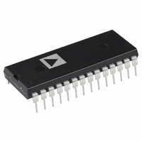
DAC8408GP Analog Devices Inc, DAC8408GP Datasheet - Page 3

DAC8408GP
Manufacturer Part Number
DAC8408GP
Description
IC DAC 8BIT QUAD W/MEMORY 28-DIP
Manufacturer
Analog Devices Inc
Datasheet
1.DAC8408FSZ-REEL.pdf
(16 pages)
Specifications of DAC8408GP
Rohs Status
RoHS non-compliant
Settling Time
190ns
Number Of Bits
8
Data Interface
Parallel
Number Of Converters
4
Voltage Supply Source
Single Supply
Operating Temperature
0°C ~ 70°C
Mounting Type
Through Hole
Package / Case
28-DIP (0.600", 15.24mm)
Power Dissipation (max)
-
REV. A
ELECTRICAL CHARACTERISTICS
DAC8408AT/BT, T
Specifications apply for DAC A, B, C, & D. Continued
Parameter
POWER SUPPLY
NOTES
1
2
3
4
5
6
ABSOLUTE MAXIMUM RATINGS
(T
V
V
I
R
I
DB0 through DB7 to DGND . . . . . . . . –0.3 V to V
Control Logic
V
Operating Temperature Range
Junction Temperature . . . . . . . . . . . . . . . . . . . . . . . . . +150 C
Storage Temperature . . . . . . . . . . . . . . . . . . . –65 C to +150 C
Lead Temperature (Soldering, 10 sec) . . . . . . . . . . . . . +300 C
This is an end-point linearity specification.
Guaranteed to be monotonic over the full operating temperature range.
ppm/ C of FSR (FSR = Full Scale Range = V
Input Resistance Temperature Coefficient = +300ppm/ C.
Logic Inputs are MOS gates. Typical input current at +25 C Is less than 10 nA.
Guaranteed by design.
OUT 1A
OUT 2A
DD
DD
REF
FB
A
Voltage Range
Supply Current
Supply Current
I
I
Input Voltage to DGND . . . . . . . . . . –0.3 V + V
I
Commercial Grade (GP) . . . . . . . . . . . . . . . . 0 C to +70 C
Industrial Grade (ET, FT, FP, FPC, FS) . –40 C to +85 C
Military Grade (AT, BT) . . . . . . . . . . . . . . –55 C to +125 C
OUT 1C
OUT 2C
OUT 2A
= +25 C, unless otherwise noted.)
A, R
to I
to DGND . . . . . . . . . . . . . . . . . . . . . . . . . . . . . . 0 V, +7 V
A, V
, I
, I
OUT 2A
FB
OUT 2B
, I
, I
, I
OUT 1B
REF
B, R
OUT 1D
OUT 2D
OUT 2B
B, V
, I
FB
,
A
,
(Not to Scale)
DAC8408
OUT 2B
= –40 C to +85 C apply for DAC8408ET/FT/FP/FPC/FS; T
C, R
REF
TOP VIEW
, I
8
9
to DGND . . . . . . . . . –0.3 V to V
to DGND . . . . . . . . . –0.3 V to V
OUT 2C
C, V
FB
, I
D to I
REF
OUT 2C
, I
D to
OUT 2D
OUT
, I
OUT 2D
. . . . . . . . . . . . . . . . .
. . . . . . . . . . . . . . . .
REF
Symbol
V
I
I
-1 LSB.)
DD
DD
DD
. . . . . . . . . . 0 V, +7 V
@ V
Conditions
T
T
DD
DD
DD
DD
A
A
DD
PIN CONNECTIONS
= +5 V; V
= +25 C
= Full Temperature Range
+ 0.3 V
+ 0.3 V
+ 0.3 V
+0.3 V
25 V
25 V
REF
–3–
=
Package Type
28-Pin Hermetic DIP (T)
28-Pin Plastic DIP (P)
28-Pin SOL (S)
28-Contact PLCC (PC)
*
CAUTION
1. Do not apply voltages higher than V
2. The digital control inputs are diode-protected; however,
3. Use proper antistatic handling procedures.
4. Absolute Maximum Ratings apply to both packaged devices
7
8
9
10
11
12
13
Specifications subject to change without notice.
A
From Digital Input to 90% of final analog output current.
All Digital Inputs “0” or V
All Digital Inputs V
stant of the final RC decay.
device in socket for cerdip and P-DIP packages;
soldered to printed circuit board for SOL and PLCC packages.
See Timing Diagram.
Digital Inputs = 0 V to V
Extrapolated: t
All Digital Inputs = 0 V; V
JA
= 0 C to +70 C apply for DAC8408GP, unless otherwise noted.
10 V; V
–0.3 V potential on any terminal except V
permanent damage may occur on unconnected inputs from
high energy electrostatic fields. Keep in conductive foam at
all times until ready to use.
and DICE. Stresses above those listed under Absolute Maxi-
mum Ratings may cause permanent damage to the device.
is specified for worst case mounting conditions, i.e.,
OUT
A, B, C, D = 0 V; T
S
(1/2 LSB) = t
IH
or V
DD
DD
IL
REF
.
.
or V
Min
4.5
PD
= +10 V.
DD
A
+ 6.2 where = the measured first time con-
= –55 C to +125 C apply for
to 0 V.
DAC8408
55
53
68
66
JA
Typ
*
DD
+0.3 V or less than
Max
5.5
50
1.0
1.5
10
27
23
29
JA
REF
JC
is specified for device
and R
JA
DAC8408
is specified for
Units
V
mA
mA
A
FB
Units
C/W
C/W
C/W
C/W
.


