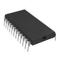
ADDAC80N-CBI-V Analog Devices Inc, ADDAC80N-CBI-V Datasheet - Page 9

ADDAC80N-CBI-V
Manufacturer Part Number
ADDAC80N-CBI-V
Description
IC DAC 12-BIT BINARY MONO 24-DIP
Manufacturer
Analog Devices Inc
Datasheet
1.ADDAC80NZ-CBI-V.pdf
(16 pages)
Specifications of ADDAC80N-CBI-V
Data Interface
Parallel
Rohs Status
RoHS non-compliant
Settling Time
2µs
Number Of Bits
12
Number Of Converters
1
Voltage Supply Source
Dual ±
Power Dissipation (max)
300mW
Operating Temperature
0°C ~ 70°C
Mounting Type
Through Hole
Package / Case
24-DIP (0.600", 15.24mm)
Resolution (bits)
12bit
Input Channel Type
Parallel
Supply Current
20mA
Digital Ic Case Style
DIP
No. Of Pins
24
Operating Temperature Range
0°C To +70°C
Msl
MSL 3 - 168 Hours
Lead Free Status / RoHS Status
Contains lead / RoHS non-compliant
Available stocks
Company
Part Number
Manufacturer
Quantity
Price
Company:
Part Number:
ADDAC80N-CBI-V
Manufacturer:
BB
Quantity:
305
Company:
Part Number:
ADDAC80N-CBI-V
Manufacturer:
BB
Quantity:
305
Part Number:
ADDAC80N-CBI-V
Manufacturer:
ADI/亚德诺
Quantity:
20 000
There are three types of drift errors over temperature: offset,
gain, and linearity. Offset drift causes a vertical translation of
the entire transfer curve; gain drift is a change in the slope of the
curve; and linearity drift represents a change in the shape of the
curve. The combination of these three drifts results in the com-
plete specification for total error over temperature.
Total error is defined as the deviation from a true straight line
transfer characteristic from exactly zero at a digital input that
calls for zero output to a point that is defined as full-scale. A
specification for total error over temperature assumes that both
the zero and full-scale points have been trimmed for zero error
at 25°C. Total error is normally expressed as a percentage of the
full-scale range. In the bipolar situation, this means the total
range from –V
Several new design concepts not previously used in DAC80-type
devices contribute to a reduction in all the error factors over
temperature. The incorporation of low temperature coefficient
silicon-chromium thin-film resistors deposited on a single chip,
a patented, fully differential, emitter weighted, precision current
steering cell structure, and a T.C. trimmed buried Zener diode
reference element results in superior wide temperature range
performance. The gain setting resistors and bipolar offset resis-
tor are also fabricated on the chip with the same SiCr material
as the ladder network, resulting in low gain and offset drift.
MONOTONICITY AND LINEARITY
The initial linearity error of ± 1/2 LSB max and the differential
linearity error of ±3/4 LSB max guarantee monotonic performance
over the specified range. It can therefore be assumed that linearity
errors are insignificant in computation of total temperature errors.
UNIPOLAR ERRORS
Temperature error analysis in the unipolar mode is straightforward:
there is an offset drift and a gain drift. The offset drift (which
comes from leakage currents and drift in the output amplifier
(OA)) causes a linear shift in the transfer curve as shown in
Figure 5. The gain drift causes a change in the slope of the
curve and results from reference drift, DAC drift, and drift in
R
BIPOLAR RANGE ERRORS
The analysis is slightly more complex in the bipolar mode. In
this mode R
amplifier (see Figure 4) to generate a current that exactly balances
the current of the MSB so that the output voltage is zero with
only the MSB on.
GAIN
relative to the DAC resistors.
BP
15V
FS
is connected to the summing node of the output
to +V
+
–
I
REF
FS
6.3V
.
6.3k
R
BP
DAC
V–
I
DAC
R
GAIN
–
+
OA
Note that if the DAC and application resistors track perfectly,
the bipolar offset drift will be zero even if the reference drifts. A
change in the reference voltage, which causes a shift in the bipolar
offset, will also cause an equivalent change in I
so that I
turned on. This effect is shown in Figure 5. The net effect of the
reference drift then is simply to cause a rotation in the transfer
around bipolar zero. However, consideration of second order
effects (which are often overlooked) reveals the errors in the
bipolar mode. The unipolar offset drifts previously discussed
will have the same effect on the bipolar offset. A mismatch of R
to the DAC resistors is usually the largest component of bipolar
drift, but in the ADDAC80 this error is held to 10 ppm/°C max.
Gain drift in the DAC also contributes to bipolar offset drift,
as well as full-scale drift, but again is held to 10 ppm/°C max.
USING THE ADDAC80 SERIES
POWER SUPPLY CONNECTIONS
For optimum performance power supply decoupling capacitors
should be added as shown in the connection diagrams. These
capacitors (1 µF electrolytic recommended) should be located
close to the ADDAC80. Electrolytic capacitors, if used, should
be paralleled with 0.01 µF ceramic capacitors for optimum high
frequency performance.
EXTERNAL OFFSET AND GAIN ADJUSTMENT
Offset and gain may be trimmed by installing external OFFSET
and GAIN potentiometers. These potentiometers should be
connected as shown in the block diagrams and adjusted as
described below. TCR of the potentiometers should be 100 ppm/°C
or less. The 3.9 MΩ and 10 MΩ resistors (20% carbon or better)
should be located close to the ADDAC80 to prevent noise pickup.
If it is not convenient to use these high-value resistors, a function-
ally equivalent “T” network, as shown in Figure 8 may be
substituted in each case. The gain adjust (Pin 23) is a high
impedance point and a 0.01 µF ceramic capacitor should be
connected from this pin to common to prevent noise pickup.
DAC
will always be exactly balanced by I
ADDAC80/ADDAC85/ADDAC87
ACTUAL
BIPOLAR (IDEAL CASE)
UNIPOLAR
OFFSET SHIFT
OFFSET (ZERO) SHIFT
INPUT
IDEAL
INPUT
GAIN SHIFT
GAIN SHIFT
REF
BP
and thus I
with the MSB
DAC
BP
,


