ADDAC80N-CBI-V Analog Devices Inc, ADDAC80N-CBI-V Datasheet
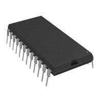
IC DAC 12-BIT BINARY MONO 24-DIP

ADDAC80N-CBI-V

Manufacturer Part Number
ADDAC80N-CBI-V
Description
IC DAC 12-BIT BINARY MONO 24-DIP
Manufacturer
Analog Devices Inc
Datasheet

Specifications of ADDAC80N-CBI-V

Data Interface
Parallel
Rohs Status
RoHS non-compliant
Settling Time
2µs
Number Of Bits
12
Number Of Converters
1
Voltage Supply Source
Dual ±
Power Dissipation (max)
300mW
Operating Temperature
0°C ~ 70°C
Mounting Type
Through Hole
Package / Case
24-DIP (0.600", 15.24mm)
Resolution (bits)
12bit
Input Channel Type
Parallel
Supply Current
20mA
Digital Ic Case Style
DIP
No. Of Pins
24
Operating Temperature Range
0°C To +70°C
Msl
MSL 3 - 168 Hours
Lead Free Status / RoHS Status
Contains lead / RoHS non-compliant

Available stocks

Company
Part Number
Manufacturer
Quantity
Price
Part Number:
ADDAC80N-CBI-V
Manufacturer:
BB
Quantity:
305
Part Number:
ADDAC80N-CBI-V
Manufacturer:
BB
Quantity:
305
Part Number:
ADDAC80N-CBI-V
Manufacturer:
ADI
Quantity:
396
Part Number:
ADDAC80N-CBI-V
Manufacturer:
ADI/亚德诺
Quantity:
20 000
a
PRODUCT DESCRIPTION
The ADDAC80 Series is a family of low cost 12-bit digital-to-
analog converters with both a high stability voltage reference
and output amplifier combined on a single monolithic chip.
The ADDAC80 Series is recommended for all low cost 12-bit D/A
converter applications where reliability and cost are of paramount
importance.
Advanced circuit design and precision processing techniques
result in significant performance advantages over conventional
DAC80 devices. Innovative circuit design reduces the total
power consumption to 300 mW, which not only improves reli-
ability, but also improves long term stability.
The ADDAC80 incorporates a fully differential, nonsaturating
precision current switching cell structure which provides greatly
increased immunity to supply voltage variation. This same struc-
ture also reduces nonlinearities due to thermal transients as the
various bits are switched; nearly all critical components operate
at constant power dissipation. High stability, SiCr thin film
resistors are trimmed with a fine resolution laser, resulting in
lower differential nonlinearity errors. A low noise, high stability,
subsurface Zener diode is used to produce a reference voltage
with excellent long term stability, high external current capabil-
ity and temperature drift characteristics which challenge the
best discrete Zener references.
The ADDAC80 Series is available in three performance grades
and three package types. The ADDAC80 is specified for use
over the 0°C to 70°C temperature range and is available in
both plastic and ceramic DIP packages. The ADDAC85 and
ADDAC87 are available in hermetically sealed ceramic packages
and are specified for the –25°C to +85°C and –55°C to +125°C
temperature ranges.
PRODUCT HIGHLIGHTS
1. The ADDAC80 series of D/A converters directly replaces all
2. Single chip construction and low power consumption pro-
3. The high speed output amplifier has been designed to settle
4. The precision buried Zener reference can supply up to 2.5 mA
5. The low TC binary ladder guarantees that all units are mono-
6. System performance upgrading is possible without redesign.
ADDAC80/ADDAC85/ADDAC87
other devices of this type with significant increases in performance.
vides the optimum choice for applications where low cost
and high reliability are major considerations.
within 1/2 LSB for a 10 V full scale transition in 2.0 µs, when
properly compensated.
for use elsewhere in the application.
tonic over the specified temperature range.
(LSB) BIT 12
(LSB) BIT 12
(MSB) BIT 1
(MSB) BIT 1
BIT 10
BIT 11
BIT 10
BIT 11
BIT 2
BIT 3
BIT 4
BIT 5
BIT 6
BIT 7
BIT 8
BIT 9
BIT 2
BIT 3
BIT 4
BIT 5
BIT 6
BIT 7
BIT 8
BIT 9
FUNCTIONAL BLOCK DIAGRAM
10
11
12
10
11
12
1
2
3
4
5
6
7
8
9
1
2
3
4
5
6
7
8
9
SWITCHES
NETWORK
SWITCHES
RESISTOR
NETWORK
RESISTOR
CURRENT
CURRENT
LADDER
LADDER
12-Bit D/A Converters
12-BIT
12-BIT
AND
AND
NC = CBI VERSIONS
NC = CBI VERSIONS
5V – CCD VERSIONS
5V – CCD VERSIONS
Complete Low Cost
5k
ADDAC80
+
CONTROL
5k
CONTROL
CIRCUIT
CIRCUIT
REF
REF
5k
6.3k
6.3k
5k
2k
24
23
22
21
20
19
18
17
16
15
14
13
24
23
22
21
20
19
18
17
16
15
14
13
GAIN ADJUST
COMMON
SCALING NETWORK
SCALING NETWORK
SCALING NETWORK
BIPOLAR OFFSET
REF INPUT
–V
NC/+V
GAIN ADJUST
COMMON
SUMMING JUNCTION
20V RANGE
10V RANGE
BIPOLAR OFFSET
REF INPUT
–V
NC/+V
V
+V
I
V
+V
V
OUT
REF
REF
OUT
S
S
S
S
OUT
OUT
L
L

Related parts for ADDAC80N-CBI-V

ADDAC80N-CBI-V Summary of contents

Page 1

PRODUCT DESCRIPTION The ADDAC80 Series is a family of low cost 12-bit digital-to- analog converters with both a high stability voltage reference and output amplifier combined on a single monolithic chip. The ADDAC80 Series is recommended for all low ...

Page 2

ADDAC80/ADDAC85/ADDAC87–SPECIFICATIONS Model TECHNOLOGY DIGITAL INPUT Binary–CBI BCD–CCD Logic Levels (TTL Compatible) V (Logic “1” (Logic “0” 5 0 TRANSFER CHARACTERISTICS ACCURACY Linearity Error @ 25°C ...

Page 3

Model TEMPERATURE RANGE Specifications Operating Storage NOTES 1 Least Significant Bit. 2 Adjustable to zero with external trim potentiometer. FSR means “Full Scale Range” and for the ± range and 10 V for the ± ...

Page 4

ADDAC80/ADDAC85/ADDAC87–SPECIFICATIONS Model ANALOG OUTPUT Voltage Models Ranges–CBI Ranges–CCD Output Current Output Impedance (dc) Short Circuit Duration Current Models Ranges–Unipolar Ranges–Bipolar Output Impedance Bipolar Unipolar Compliance Internal Reference Voltage ( Output Impedance 6 Max External Current Tempco of Drift ...

Page 5

Model TECHNOLOGY DIGITAL INPUT Binary–CBI BCD–CCD Logic Levels (TTL Compatible) V (Logic “1” (Logic “0” 5 0 TRANSFER CHARACTERISTICS ACCURACY Linearity Error @ 25°C CBI ...

Page 6

ADDAC80/ADDAC85/ADDAC87–SPECIFICATIONS Model POWER SUPPLY REQUIREMENTS Rated Voltages Range Analog Supplies Logic Supplies 7 Supply Drain +15 V – TEMPERATURE RANGE Specification Operating Storage NOTES 1 Least Significant Bit. 2 Adjustable to zero with external trim potentiometer. ...

Page 7

... Input Model Code ADDAC80N-CBI-V Binary ADDAC80D-CBI-V Binary ADDAC85D-CBI-V Binary ADDAC87D-CBI-V Binary ADDAC80-CBI-V Binary ADDAC80-CBI-I Binary ADDAC80-CCD-V Binary Coded Decimal ADDAC80-CCD-I Binary Coded Decimal 2 ADDAC80Z-CBI-V Binary 2 ADDAC80Z-CBI-I Binary 2 ADDAC80Z-CCD-V Binary Coded Decimal 2 ADDAC80Z-CCD-I Binary Coded Decimal 3 ADDAC85C-CBI-V Binary ADDAC85C-CBI-I Binary 3 ADDAC85-CBI-V Binary ...

Page 8

ADDAC80/ADDAC85/ADDAC87 ACCURACY Accuracy error of a D/A converter is the difference between the analog output that is expected when a given digital code is applied and the output that is actually measured with that code applied to the converter. Accuracy ...

Page 9

6.3V 6.3k – I REF DAC V– There are three types of drift errors over temperature: offset, gain, and linearity. Offset drift causes a vertical translation of the entire transfer curve; gain drift is a change ...

Page 10

ADDAC80/ADDAC85/ADDAC87 1 24 REF 2 23 CONTROL CIRCUIT 12-BIT 5 20 RESISTOR 2k LADDER 6 19 NETWORK 3k 7 AND 18 CURRENT SWITCHES 6. Offset ...

Page 11

VOLTAGE OUTPUT MODELS Internal scaling resistors provided in the ADDAC80 may be connected to produce bipolar output voltage ranges of ± ± ± 2 unipolar output voltage ranges ...

Page 12

ADDAC80/ADDAC85/ADDAC87 DRIVING A RESISTOR LOAD BIPOLAR The equivalent output circuit for a bipolar output voltage range is shown in Figure 13   × Ω ...

Page 13

Table V. External Op Amp Voltage Mode Connections Output Digital Connect Range Input Codes A to ± COB or CTC 19 ± COB or CTC 18 ± 2.5 V COB or CTC ...

Page 14

ADDAC80/ADDAC85/ADDAC87 24-Lead Side Brazed Ceramic DIP for Hybrid (DH-24A) 0.005 (0.13) MIN 24 PIN 1 SEE NOTE 1 0.225 (5.72) MAX 0.200 (5.08) 0.120 (3.05) 0.023 (0.58) 0.014 (0.36) NOTES 1. INDEX AREA; A NOTCH OR A LEAD ONE IDENTIFICATION ...

Page 15

Revision History Location Data Sheet changed from REV REV. B. Update OUTLINE DIMENSION drawings . . . . . . . . . . . . . . . . . . . . . . . . ...

Page 16

...

Related keywords