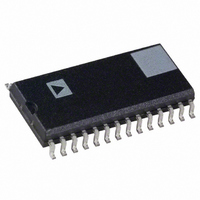
AD7564AR-B Analog Devices Inc, AD7564AR-B Datasheet - Page 3

AD7564AR-B
Manufacturer Part Number
AD7564AR-B
Description
IC DAC 12BIT QUAD 3.3V LP 28SOIC
Manufacturer
Analog Devices Inc
Datasheet
1.AD7564BRSZ.pdf
(16 pages)
Specifications of AD7564AR-B
Rohs Status
RoHS non-compliant
Settling Time
500ns
Number Of Bits
12
Data Interface
Serial
Number Of Converters
4
Voltage Supply Source
Single Supply
Power Dissipation (max)
50µW
Operating Temperature
-40°C ~ 85°C
Mounting Type
Surface Mount
Package / Case
28-SOIC (7.5mm Width)
Biased Mode
Parameter
ACCURACY
DIGITAL INPUTS
DIGITAL OUTPUT (SDOUT)
POWER REQUIREMENTS
NOTES
1
2
3
Specifications subject to change without notice.
(for example: AD7564AR-B). Figure 19 is an example of Biased Mode Operation.
These specifications apply with the devices biased up at 1.23 V for single supply applications. The model numbering reflects this by means of a "-B" suffix
Temperature ranges is as follows: A Version: –40 C to +85 C.
Not production tested. Guaranteed by characterization at initial product release.
Resolution
Relative Accuracy
Differential Nonlinearity
Gain Error
Gain Temperature Coefficient
Output Leakage Current
Input Resistance
V
V
V
V
I
C
Output Low Voltage (V
Output Low Voltage (V
Output High Voltage (V
Output High Voltage (V
V
Power Supply Sensitivity
I
INH
DD
INH
INH
INL
INL
DD
IN
REV. A
+25 C
T
I
@ +25 C
T
@ I
OUT1
, Input Capacitance
Gain/ V
MIN
MIN
, Input Current
, Input Low Voltage @ V
, Input Low Voltage @ V
, Input High Voltage @ V
, Input High Voltage @ V
Range
OUT2
to T
to T
Pins
DD
MAX
MAX
1
(V
T
MAX
DD
3
OL
OL
, unless otherwise noted)
OH
OH
= +3 V to +5.5 V; V
3
)
)
)
)
DD
DD
3
DD
DD
= +5 V
= +3.3 V
= +5 V
= +3.3 V
IOUT1
= V
A Grade
12
2
5
10
50
6
2.4
2.1
0.8
0.6
10
0.4
0.2
4.0
V
3/5.5
–75
10
IOUT2
1
0.9
4
5
1
DD
= 1.23 V; AGND = 0 V; V
– 0.2
2
Units
Bits
LSB max
LSB max
LSBs max
LSBs max
ppm FSR/ C typ
ppm FSR/ C max
nA max
nA max
k min
V min
V min
V max
V max
pF max
V max
V max
V min
V min
V min/V max
dB typ
A max
A max
–3–
REF
= 0 V to 2.45 V; T
Test Conditions/Comments
1 LSB = (V
V
All Grades Guaranteed Monotonic Over
Temperature
See Terminology Section
This Varies with DAC Input Code
Load Circuit as in Figure 2.
V
V
V
V
V
SDOUT Open Circuit
I
V
SDOUT Open Circuit
DD
IOUT2
DD
DD
DD
DD
INH
INH
is typically 2 mA with V
= +5 V
= +3.3 V
= +5 V
= +3.3 V
= V
= 2.4 V min, V
= 1.23 V and V
A
DD
= T
IOUT2
– 0.1 V min, V
MIN
to
– V
REF
INL
REF
)/2
= 0.8 V max;
12
= 0 V
INL
DD
= 300 V when
= 0.1 V max;
= +5 V,
AD7564


