AD667JN Analog Devices Inc, AD667JN Datasheet - Page 4
AD667JN
Manufacturer Part Number
AD667JN
Description
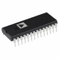
IC DAC 12BIT V-OUT 28-DIP
Manufacturer
Analog Devices Inc
Datasheet
1.AD667JNZ.pdf
(8 pages)
Specifications of AD667JN
Settling Time
3µs
Rohs Status
RoHS non-compliant
Number Of Bits
12
Number Of Converters
1
Voltage Supply Source
Dual ±
Power Dissipation (max)
1W
Operating Temperature
0°C ~ 70°C
Mounting Type
Through Hole
Package / Case
28-DIP (0.600", 15.24mm)
Resolution (bits)
12bit
Data Interface
CMOS, Byte, Nibble, Parallel, TTL
Digital Ic Case Style
DIP
No. Of Pins
28
Operating Temperature Range
0°C To +70°C
Update Rate
0.5MSPS
Package
28PDIP W
Resolution
12 Bit
Conversion Rate
500 KSPS
Architecture
Current Steering
Digital Interface Type
Parallel
Number Of Outputs Per Chip
1
Output Type
Voltage
Full Scale Error
±0.2 %FSR
Integral Nonlinearity Error
±0.75 LSB
Maximum Settling Time
4 us
Lead Free Status / RoHS Status
Contains lead / RoHS non-compliant
Available stocks
Company
Part Number
Manufacturer
Quantity
Price

Part Number:
AD667JN
Manufacturer:
ADI/亚德诺
Quantity:
20 000
Company:
Part Number:
AD667JNZ
Manufacturer:
PSPR
Quantity:
6 220
Part Number:
AD667JNZ
Manufacturer:
ADI/亚德诺
Quantity:
20 000


AD667
Model
AD667JN
AD667JP
AD667KN
AD667KP
AD667AD
AD667BD
AD667SD
AD667SE
AD667/883B –55 to +125
NOTES
*Refer to AD667/883B military data sheet.
1
2
THE AD667 OFFERS TRUE 12-BIT PERFORMANCE
OVER THE FULL TEMPERATURE RANGE
LINEARITY ERROR: Analog Devices defines linearity error as
the maximum deviation of the actual, adjusted DAC output
Output
Range
0 V to +10 V
0 V to +5 V
For details on grade and package offerings screened in accordance with MIL-STD-
D = Ceramic DIP; E = Leadless Ceramic Chip Carrier; N = Plastic DIP;
883, refer to the Analog Devices Military Products Databook or current AD667/
883B data sheet.
P = Plastic Leaded Chip.
10 V
5 V
2.5 V
l
Temperature
Range— C
0 to +70
0 to +70
0 to +70
0 to +70
25 to +85
–25 to +85
–55 to +125
–55 to +125
Digital
Input Codes
Offset Binary
Offset Binary
Offset Binary
Straight Binary
Straight Binary
ORDERING GUIDE
PLCC, LCC
Linearity
Error Max TC Max
@ +25 C
*
1/2 LSB
1/2 LSB
1/4 LSB
1/4 LSB
1/2 LSB
1/4 LSB
1/2 LSB
1/2 LSB
Gain
ppm/ C Package Option
30
30
15
15
30
15
30
30
*
Connect
Pin 9 to
1
1 and 2
2
1 and 2
2
Table I. Output Voltage Range Connections
Plastic DIP (N-28)
PLCC (P-28A)
Plastic DIP (N-28)
PLCC (P-28A)
Ceramic DIP (D-28)
Ceramic DIP (D-28)
Ceramic DIP (D-28)
LCC (E-28A)
*
Connect
Pin 1 to
9
2 and 9
3
2 and 9
3
PIN CONNECTIONS
2
–4–
Connect
Pin 2 to
NC
1 and 9
9
1 and 9
9
from the ideal analog output (a straight line drawn from 0 to FS
– 1 LSB) for any bit combination. The AD667 is laser trimmed
to 1/4 LSB (0.006% of FS) maximum error at +25 C for the K
and B versions and 1/2 LSB for the J, A and S versions.
MONOTONICITY: A DAC is said to be monotonic if the
output either increases or remains constant for increasing digital
inputs such that the output will always be a nondecreasing func-
tion of input. All versions of the AD667 are monotonic over
their full operating temperature range.
DIFFERENTIAL NONLINEARITY: Monotonic behavior re-
quires that the differential linearity error be less than 1 LSB
both at +25 C and over the temperature range of interest. Dif-
ferential nonlinearity is the measure of the variation in analog
value, normalized to full scale, associated with a 1 LSB change
in digital input code. For example, for a 10 volt full-scale out-
put, a change of 1 LSB in digital input code should result in a
2.44 mV change in the analog output (1 LSB = 10 V 1/4096 =
2.44 mV). If in actual use, however, a 1 LSB change in the
input code results in a change of only 0.61 mV (1/4 LSB) in
analog output, the differential linearity error would be –1.83 mV,
or –3/4 LSB. The AD667K and B grades have a max differential
linearity error of 1/2 LSB, which specifies that every step will be
at least 1/2 LSB and at most 1 1/2 LSB.
Connect
Pin 4 to
6 (Through 50
6 (Through 50
6 (Through 50
5 (or Optional Trim—See Figure 2)
5 (or Optional Trim—See Figure 2)
DIP
Fixed or 100
Fixed or 100
Fixed or 100
Trim Resistor)
Trim Resistor)
Trim Resistor)
REV. A
Related parts for AD667JN
Image
Part Number
Description
Manufacturer
Datasheet
Request
R

Part Number:
Description:
±1.7g Dual-Axis IMEMS Accelerometer Evaluation Board
Manufacturer:
Analog Devices Inc
Datasheet:

Part Number:
Description:
Inertial Sensor Evaluation System
Manufacturer:
Analog Devices Inc
Datasheet:
Part Number:
Description:
Manufacturer:
Analog Devices Inc
Datasheet:
Part Number:
Description:
Manufacturer:
Analog Devices Inc
Datasheet:
Part Number:
Description:
Manufacturer:
Analog Devices Inc
Datasheet:
Part Number:
Description:
Manufacturer:
Analog Devices Inc
Datasheet:
Part Number:
Description:
Manufacturer:
Analog Devices Inc
Datasheet:
Part Number:
Description:
Manufacturer:
Analog Devices Inc
Datasheet:
Part Number:
Description:
Manufacturer:
Analog Devices Inc
Datasheet:
Part Number:
Description:
Manufacturer:
Analog Devices Inc
Datasheet:
Part Number:
Description:
Manufacturer:
Analog Devices Inc
Datasheet:
Part Number:
Description:
Manufacturer:
Analog Devices Inc
Datasheet:
Part Number:
Description:
Manufacturer:
Analog Devices Inc
Datasheet: