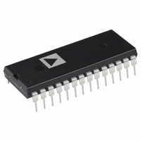
AD667JN Analog Devices Inc, AD667JN Datasheet

AD667JN
Specifications of AD667JN
Available stocks
Related parts for AD667JN
AD667JN Summary of contents
Page 1
...
Page 2
AD667–SPECIFICATIONS Model DIGITAL INPUTS Resolution Logic Levels (TTL, Compatible, T –T MIN MAX V (Logic “l’’ (Logic “0” 5 0 TRANSFER CHARACTERISTICS ACCURACY Linearity Error ...
Page 3
Model DIGITAL INPUTS Resolution 1 Logic Levels (TTL, Compatible, T –T ) MIN MAX V (Logic “l’’ (Logic “0” 5 0 TRANSFER CHARACTERISTICS ACCURACY Linearity ...
Page 4
... AD667 PLCC, LCC ORDERING GUIDE Linearity Gain Temperature Error Max TC Max l Model Range— +25 C ppm/ C Package Option AD667JN 0 to +70 1/2 LSB 30 AD667JP 0 to +70 1/2 LSB 30 AD667KN 0 to +70 1/4 LSB 15 AD667KP 0 to +70 1/4 LSB 15 AD667AD 25 to +85 1/2 LSB 30 AD667BD –25 to +85 ...
Page 5
ANALOG CIRCUIT CONNECTIONS Internal scaling resistors provided in the AD667 may be connected to produce bipolar output voltage ranges unipolar output voltage ranges ...
Page 6
AD667 Small resistors may be added to the feedback resistors in order to accomplish small modifications in the scaling. For example 10.24 V full scale is desired, a 140 1% low TC metal-film resistor can be added in ...
Page 7
Figure 5. AD667 Block Diagram It is permissible to enable more than one of the latches simulta- neously first rank latch is enabled coincident with the sec- ond rank latch, the data will reach the second rank correctly ...
Page 8
AD667 Right-justified data can be similarly accommodated. The over- lapping of data lines is reversed, and the address connections are slightly different. The AD667 still occupies two adjacent locations in the processor’s memory map. In the circuit of Fig- ure ...


