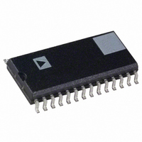
AD7805CR Analog Devices Inc, AD7805CR Datasheet - Page 23

AD7805CR
Manufacturer Part Number
AD7805CR
Description
IC DAC 10BIT QUAD PARALL 28-SOIC
Manufacturer
Analog Devices Inc
Datasheet
1.AD7808BRZ.pdf
(28 pages)
Specifications of AD7805CR
Rohs Status
RoHS non-compliant
Settling Time
1.5µs
Number Of Bits
10
Data Interface
Parallel
Number Of Converters
4
Voltage Supply Source
Analog and Digital
Power Dissipation (max)
66mW
Operating Temperature
-40°C ~ 85°C
Mounting Type
Surface Mount
Package / Case
28-SOIC (7.5mm Width)
Available stocks
Company
Part Number
Manufacturer
Quantity
Price
Part Number:
AD7805CR
Manufacturer:
ADI/亚德诺
Quantity:
20 000
REV. A
AD7805/AD7809–ADSP-2101 Interface
Figure 38 shows a parallel interface between the AD7805/AD7809
and the ADSP-2101/ADSP-2103 digital signal processor.
Fast interface timing allows the AD7805/AD7809 interface
directly to the DSP. In this interface an external timer is used to
update the DACs.
Data is loaded to the AD7805/AD7809 input register using the
following instruction:
MR0 = ADSP-2101 MR0 Register.
DAC = Decoded DAC Address.
AD7805/AD7809–TMS32020 Interface
Figure 39 shows a parallel interface between the AD7805/AD7809
and the TMS32020 processor.
DM(DAC) = MR0,
Figure 38. AD7805/AD7809–ADSP-2101/ADSP-2103
Interface
ADSP-2101*/
ADSP-2103*
TMS32020
Figure 39. AD7805/AD7809–TMS32020 Interface
DMA14
DMD15
DMA0
DMD0
STRB
DMS
R/W
A15
D15
WR
A0
D0
IS
**ADDITIONAL PINS OMITTED FOR CLARITY
**A2 CONTAINED ON THE AD7809 ONLY
**ADDITIONAL PINS OMITTED FOR CLARITY
**A2 CONTAINED ON THE AD7809 ONLY
ADDRESS BUS
EN
ADDRESS BUS
EN
DECODE
DECODE
ADDR
ADDR
DATA BUS
DATA BUS
TIMER
LDAC
CS
WR
DB9
DB0
CS
LDAC
WR
DB9
DB0
A0
AD7805*/
AD7805*/
AD7809
AD7809
A0 A1
A1
MODE
A2**
A2**
–23–
Again fast interface timing allows the AD7805/AD7809 inter-
face directly to the processor. Data is loaded to the AD7805/
AD7809 input latch using the following instruction:
DAC = Decoded DAC Address.
D = Data Memory Address.
Certain applications may require that the updating of the DAC
latch be controlled by the microprocessor rather than the exter-
nal timer. One option as shown in the TMS32020 interface is to
decode the LDAC from the address bus so that a write opera-
tion to the DAC latch (at a separate address to the input latch)
updates the output.
AD7805/AD7809–8051/8088 Interface
Figure 40 shows a parallel interface between the AD7805/
AD7809 and the 8051/8088 processors.
OUT DAC, D.
8051/8088
PSEN OR DEN
Figure 40. AD7805/AD7809–8051/8088 Interface
AD7804/AD7805/AD7808/AD7809
ALE
AD7
AD0
A15
WR
A8
**ADDITIONAL PINS OMITTED FOR CLARITY
**A2 CONTAINED ON THE AD7809 ONLY
OCTAL
LATCH
ADDRESS/DATA BUS
ADDRESS BUS
EN
DECODE
ADDR
CS
LDAC
WR
DB9
DB0
AD7805*/
AD7809
A0
A1
MODE
A2**


