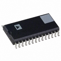
AD7805CR Analog Devices Inc, AD7805CR Datasheet - Page 13

AD7805CR
Manufacturer Part Number
AD7805CR
Description
IC DAC 10BIT QUAD PARALL 28-SOIC
Manufacturer
Analog Devices Inc
Datasheet
1.AD7808BRZ.pdf
(28 pages)
Specifications of AD7805CR
Rohs Status
RoHS non-compliant
Settling Time
1.5µs
Number Of Bits
10
Data Interface
Parallel
Number Of Converters
4
Voltage Supply Source
Analog and Digital
Power Dissipation (max)
66mW
Operating Temperature
-40°C ~ 85°C
Mounting Type
Surface Mount
Package / Case
28-SOIC (7.5mm Width)
Available stocks
Company
Part Number
Manufacturer
Quantity
Price
Part Number:
AD7805CR
Manufacturer:
ADI/亚德诺
Quantity:
20 000
REV. A
of the Main DAC to the bottom of the transfer function, V
With twos complement coding the output of the DAC is cleared
to midscale which is V
output of the Sub DAC to midscale thus the output of the Sub
DAC makes zero contribution to the output of the channel.
AD7805/AD7809 CONTROL REGISTERS
Access to the control registers of the AD7805/AD7809 is
achieved by taking the mode pin to a logic low. The control
register of these DACs are configured as in Figures 12 and 13.
There are two control registers associated with the part. System
control register which looks after the input coding, data format,
power down, system clear and system standby. The channel
control register contains bits that affect the operation of the
selected DAC. The external address bits are used to select the
DACs. These registers are eight bits wide and the last two bits
are control bits. The mode pin must be low to have access to the
control registers.
DB9
X = Don’t Care
Figure 12. AD7805/AD7809 System Control Register Con-
figuration, (MODE = 0)
DB9
X = Don’t Care
Figure 13. AD7805/AD7809 Channel Control Register Con-
figuration (MODE = 0)
The external mode pin must be taken high to allow data to be
written to the DAC data registers. Figure 14 shows the bit allo-
cations when 10-bit parallel operation is selected in the system
control register.
MX1 MX0 MAIN/SUB X
X X 10/8 BIN/COMP
INTERNAL V
REGISTER
CHANNELS
CONTROL
CHANNEL
SYSTEM
TO ALL
SINGLE
Figure 11. AD7805/AD7809 Internal Registers
REFIN
V
V
DD
OUT
REF
/2
MODE ADDR
DECODER
MUX
REGISTER
CHANNEL
CONTROL
BIAS
V
. A hardware clear always clears the
BIAS
PD SSTBY SCLR 0
INPUT REGISTER
X
D9 D2 D1 D0
DATA REGISTER
DAC REGISTER
STBY CLR 0
10-BIT DAC
(MAIN DAC)
10
10
CONTROL
DB2
DB2 DB1
LOGIC
DATA REGISTER
DAC REGISTER
X
8-BIT DAC
(SUB DAC)
X
DB1
8
8
MD0 = 0
MD0 = 1
BIAS
CS
WR
LDAC
DB0
DB0
/16.
–13–
DB9
X = Don’t Care
Figure 14. AD7805/AD7809 Main DAC Data Register (Top)
and Sub DAC Data Register (Bottom) Configuration
(MODE = 1, 10 /8 = 0)
Figure 15 shows the bit allocations when 8-bit parallel operation
is selected in the system control register. DB9 to DB2 are re-
tained as data bits. DB1 acts as a high byte or low byte enable.
When DB1 is low, the eight MSBs of the data word are loaded
to the input register. When DB1 is high, the low byte consisting
of the two LSBs are loaded to the input register. DB0 is used to
select either the Main or Sub DAC when in the byte mode.
DB9
X = Don’t Care
Figure 15. AD7805/AD7809 Main DAC Data Register Con-
figuration (MODE = 1, 10 /8 = 1, MAIN /SUB = 0)
Figure 16 shows the bit allocations for writing to the Sub DAC.
DB9
X = Don’t Care
Figure 16. AD7805/AD7809 Sub DAC Data Register Con-
figuration (MODE = 1, MAIN /SUB = 1)
Each DAC has a separate channel control register. The follow-
ing is a brief discussion on the bits in each of the control registers.
DAC Selection (A2, A1, A0)
The external address pins in conjunction with CS, WR and
MODE are used to address the various DAC data and control
registers. Table IVa shows how these DAC registers can be
addressed on the AD7805. Table IVb shows how these registers
are addressed on the AD7809. Refer to Figures 12 to 16 for infor-
mation on the registers.
MODE
0
0
0
0
1
1
1
1
DB9 DB8 DB7 DB6 DB5 DB4 DB3 DB2 DB1
DB7 DB6 DB5 DB4 DB3 DB2 DB1 DB0
DB9 DB8 DB7 DB6 DB5 DB4 DB3 DB2
DB7 DB6 DB5 DB4 DB3 DB2 DB1 DB0
X
Table IVa. AD7805 DAC Data/Control Register
Selection Table
AD7804/AD7805/AD7808/AD7809
X
X
A1
0
0
1
1
0
0
1
1
X
X
A0
0
1
0
1
0
1
0
1
X
DB1 DB0
Function Selected
DAC A Control Registers
DAC B Control Registers
DAC C Control Registers
DAC D Control Registers
DAC A Data Registers
DAC B Data Registers
DAC C Data Registers
DAC D Data Registers
DB2
DB2 DB1
DB1
0 MAIN/SUB
1 MAIN/SUB
X MAIN/SUB
X
DB0
DB0
DB0
DB0
X


