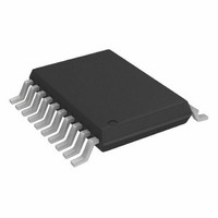
DAC8562FRU Analog Devices Inc, DAC8562FRU Datasheet - Page 3

DAC8562FRU
Manufacturer Part Number
DAC8562FRU
Description
IC DAC 12BIT PARALLEL 5V 20TSSOP
Manufacturer
Analog Devices Inc
Datasheet
1.DAC8562FSZ.pdf
(16 pages)
Specifications of DAC8562FRU
Rohs Status
RoHS non-compliant
Settling Time
16µs
Number Of Bits
12
Data Interface
Parallel
Number Of Converters
1
Voltage Supply Source
Single Supply
Power Dissipation (max)
30mW
Operating Temperature
-40°C ~ 85°C
Mounting Type
Surface Mount
Package / Case
20-TSSOP
REV. A
ABSOLUTE MAXIMUM RATINGS*
V
Logic Inputs to DGND . . . . . . . . . . . . . . . –0.3 V, V
V
V
AGND to DGND . . . . . . . . . . . . . . . . . . . . . . . . . –0.3 V, V
I
Package Power Dissipation . . . . . . . . . . . . . . (T
Thermal Resistance
Maximum Junction Temperature (T
Operating Temperature Range . . . . . . . . . . . . . –40 C to +85 C
Storage Temperature Range . . . . . . . . . . . . . –65 C to +150 C
Lead Temperature (Soldering, 10 secs) . . . . . . . . . . . . +300 C
*Stresses above those listed under “Absolute Maximum Ratings” may cause
WAFER TEST LIMITS
Parameter
STATIC PERFORMANCE
LOGIC INPUTS
SUPPLY CHARACTERISTICS
NOTE
1
CAUTION
ESD (electrostatic discharge) sensitive device. The digital control inputs are diode protected;
however, permanent damage may occur on unconnected devices subject to high energy electrostatic
fields. Unused devices must be stored in conductive foam or shunts. The protective foam should be
discharged to the destination socket before devices are inserted.
permanent damage to the device. This is a stress rating only and functional
operation of the device at these or any other conditions above those indicated in the
operational sections of this specification is not implied. Exposure to absolute
maximum rating conditions for extended periods may affect device reliability.
OUT
Electrical tests are performed at wafer probe to the limits shown. Due to variations in assembly methods and normal yield loss, yield after packaging is not guaranteed
for standard product dice. Consult factory to negotiate specifications based on dice lot qualifications through sample lot assembly and testing.
DD
OUT
REFOUT
20-Pin Plastic DIP Package (P) . . . . . . . . . . . . . . . . 74 C/W
20-Lead SOIC Package (S) . . . . . . . . . . . . . . . . . . . 89 C/W
Relative Accuracy
Differential Nonlinearity
Zero-Scale Error
Full-Scale Voltage
Reference Output Voltage
Logic Input Low Voltage
Logic Input High Voltage
Input Leakage Current
Positive Supply Current
Power Dissipation
Power Supply Sensitivity
to DGND and AGND . . . . . . . . . . . . . . . . –0.3 V, +10 V
Short Circuit to GND . . . . . . . . . . . . . . . . . . . . . . 50 mA
to AGND . . . . . . . . . . . . . . . . . . . . . –0.3 V, V
to AGND . . . . . . . . . . . . . . . . . . –0.3 V, V
JA
(@ V
unless otherwise noted)
DD
J
max) . . . . . . . . . . 150 C
= +5.0 V
Symbol
INL
DNL
V
V
V
V
V
I
I
P
PSS
IL
DD
DISS
ZSE
FS
REF
IL
IH
J
5%, R
max – T
DD
DD
DD
Condition
No Missing Codes
Data = 000
Data = FFF
V
V
V
V
V
L
IH
IL
IH
IL
= No Load, T
DD
+ 0.3 V
+ 0.3 V
+ 0.3 V
= 0 V, V
= 0 V, V
= 2.4 V, V
= 2.4 V, V
A
)/
= 5%
DD
JA
–3–
H
H
DD
DD
A
IL
IL
= +5 V
= +5 V
= +25 C, applies to part number DAC8562GBC only,
= 0.8 V
= 0.8 V
DB
V
CE
H
L
X
H
CLR
11–0
OUT
CE
+ Positive Logic Transition; X Don't Care.
+
FS
ZS
1
0
1
0
0
1
Table I. Control Logic Truth Table
Min
–1
–1
4.085
2.490
2.4
CLR
H
H
H
L
Figure 2. Timing Diagram
+
t
CEW
t
DS
DATA VALID
t
S
Typ
+1/2
4.095
2.500
3
0.6
15
3
0.002
3/4
3/4
DAC Register Function
Latched
Transparent
Latched with New Data
Loaded with All Zeros
Latched All Zeros
t
±1 LSB
ERROR BAND
DH
WARNING!
Max
+1
+ 1
+3
4.105
2.510
0.8
10
6
1
30
5
0.004
ESD SENSITIVE DEVICE
t
CLRW
DAC8562
t
S
LSB
Units
LSB
LSB
V
V
V
V
mA
mA
mW
mW
%/%
A


