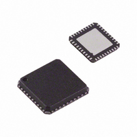
AD9116BCPZ Analog Devices Inc, AD9116BCPZ Datasheet - Page 49

AD9116BCPZ
Manufacturer Part Number
AD9116BCPZ
Description
IC DAC DUAL 12BIT LO PWR 40LFCSP
Manufacturer
Analog Devices Inc
Series
TxDAC®r
Datasheet
1.AD9114BCPZ.pdf
(80 pages)
Specifications of AD9116BCPZ
Data Interface
Serial
Number Of Bits
12
Number Of Converters
2
Voltage Supply Source
Analog and Digital
Power Dissipation (max)
232mW
Operating Temperature
-40°C ~ 85°C
Mounting Type
Surface Mount
Package / Case
40-LFCSP
Resolution (bits)
12bit
Sampling Rate
125MSPS
Input Channel Type
Serial
Supply Current
55mA
Digital Ic Case Style
CSP
No. Of Pins
40
Lead Free Status / RoHS Status
Lead free / RoHS Compliant
Settling Time
-
Lead Free Status / RoHS Status
Lead free / RoHS Compliant, Lead free / RoHS Compliant
Available stocks
Company
Part Number
Manufacturer
Quantity
Price
Company:
Part Number:
AD9116BCPZ
Manufacturer:
ADI
Quantity:
250
Two registers are assigned to each DAC with 10 bits for the
actual DAC current to be generated, a 3-bit offset (and gain)
adjustment, a 2-bit current range adjustment, and an enable/
disable bit. Setting the QAUXOFS (Register 0x0A) and
IAUXOFS (Register 0x0C) bits to all 1s disables the respective
op amp and routes the DAC current directly to the respective
FSADJI/AUXI or FSADJQ/AUXQ pins. This is especially useful
when the loads to be driven are beyond the limited capability of
the on-chip amplifier.
When not enabled (QAUXEN or IAUXEN = 0), the respective
DAC output is in open circuit.
DAC-TO-MODULATOR INTERFACING
The auxiliary DACs can be used for local oscillator (LO)
cancellation when the DAC output is followed by a quadrature
modulator. This LO feedthrough is caused by the input referred
dc offset voltage of the quadrature modulator (and the DAC
output offset voltage mismatch) and can degrade system
performance. Typical DAC-to-quadrature modulator interfaces
are shown in Figure 107 and Figure 108, with the series resistor
value chosen to give an appropriate adjustment range. Figure 107
also shows external load resistors in use. Often, the input common-
mode voltage for the modulator is much higher than the output
compliance range of the DAC, so that ac coupling or a dc level
shift is necessary. If the required common-mode input voltage
on the quadrature modulator matches that of the DAC, the dc
blocking capacitors in Figure 107 can be removed and the on-chip
resistors can be connected.
Figure 108 shows a greatly simplified circuit that takes full
advantage of the internal components supplied in the DAC.
A low-pass or band-pass passive filter is recommended when
spurious signals from the DAC (distortion and DAC images) at the
quadrature modulator inputs can affect the system performance. In
the example shown in Figure 108, the filter must be able to pass dc
to properly bias the modulator. Placing the filter at the location
shown in Figure 107 and Figure 108 allows easy design of the filter,
because the source and load impedances can easily be designed
close to 50 Ω for a 20 mA full-scale output. When the resistance
at the modulator inputs is known, an optimum value for the
series resistor can be calculated from the modulator input
offset voltage ratings.
AD9114/AD9115/
AD9116/AD9117
AD9114/AD9115/
AD9116/AD9117
AUXDAC1
I DAC
Figure 107. Typical Use of Auxiliary DACs
50Ω
0.1µF
0.1µF
50Ω
OPTIONAL
FILTERING
PASSIVE
100kΩ
5kΩ
TO
MODULATOR V+
QUADRATURE
MODULATOR
I OR Q
INPUTS
Rev. A | Page 49 of 80
CORRECTING FOR NONIDEAL PERFORMANCE OF
QUADRATURE MODULATORS ON THE IF-TO-RF
CONVERSION
Analog quadrature modulators make it very easy to realize
single sideband radios. These DACs are most often used to make
radio transmitters, such as in cell phone towers. However, there
are several nonideal aspects of quadrature modulator performance.
Among these analog degradations are gain mismatch and LO
feedthrough.
Gain Mismatch
The gain in the real and imaginary signal paths of the quadrature
modulator may not be matched perfectly. This leads to less than
optimal image rejection because the cancellation of the negative
frequency image is less than perfect.
LO Feedthrough
The quadrature modulator has a finite dc referred offset, as well
as coupling from its LO port to the signal inputs. These can lead
to a significant spectral spur at the frequency of the quadrature
modulator LO.
The AD9114/AD9115/AD9116/AD9117 have the capability to
correct for both of these analog degradations. However, understand
that these degradations drift over temperature; therefore, if close to
optimal single sideband performance is desired, a scheme for
sensing these degradations over temperature and correcting
them may be necessary.
I/Q CHANNEL GAIN MATCHING
Fine gain matching is achieved by adjusting the values in the DAC
fine gain adjustment registers. For the I DAC, these values are in
the I DAC Gain register (Register 0x03, I DACGAIN[5:0]). For the
Q DAC, these values are in the Q DAC gain register (Register 0x06,
Q DACGAIN[5:0]). These are 6-bit values that cover ±2% of full
scale. To perform gain compensation by starting from the default
values of zero, raise the value of one of these registers a few steps
until it can be determined if the amplitude of the unwanted
image is increased or decreased. If the unwanted image increases in
amplitude, remove the step and try the same adjustment on the
other DAC control register. Iterate register changes until the
rejection cannot be improved further. If the fine gain adjustment
range is not sufficient to find a null (that is, the register goes full
scale with no null apparent), adjust the course gain settings of the
two DACs accordingly and try again. Variations on this simple
method are possible.
Figure 108. Typical Use of Auxiliary DACs When DC Coupling to Quadrature
AD9114/AD9115/
AD9116/AD9117
AD9114/AD9115/
AD9116/AD9117
AUXDAC
I OR Q DAC
AD9114/AD9115/AD9116/AD9117
50Ω
Modulator ADL537x Family
50Ω
LOW- PASS
OPTIONAL
FILTERING
5kΩ
100Ω
ADL5370
FAMILY
I OR Q INPUTS


