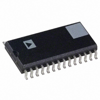
AD9762AR Analog Devices Inc, AD9762AR Datasheet - Page 6

AD9762AR
Manufacturer Part Number
AD9762AR
Description
IC DAC 12BIT 125MSPS 28-SOIC
Manufacturer
Analog Devices Inc
Series
TxDAC®r
Datasheet
1.AD9762ARUZ.pdf
(23 pages)
Specifications of AD9762AR
Rohs Status
RoHS non-compliant
Settling Time
35ns
Number Of Bits
12
Data Interface
Parallel
Number Of Converters
1
Voltage Supply Source
Analog and Digital
Power Dissipation (max)
160mW
Operating Temperature
-40°C ~ 85°C
Mounting Type
Surface Mount
Package / Case
28-SOIC (7.5mm Width)
Package
28SOIC W
Resolution
12 Bit
Conversion Rate
125 MSPS
Architecture
Segment
Digital Interface Type
Parallel
Number Of Outputs Per Chip
1
Output Type
Current
Full Scale Error
10 %FSR
Integral Nonlinearity Error
±4 LSB
Maximum Settling Time
0.035(Typ) us
Number Of Channels
1
Interface Type
Parallel
Single Supply Voltage (typ)
5V
Dual Supply Voltage (typ)
Not RequiredV
Power Supply Requirement
Analog and Digital
Single Supply Voltage (min)
2.7V
Single Supply Voltage (max)
5.5V
Dual Supply Voltage (min)
Not RequiredV
Dual Supply Voltage (max)
Not RequiredV
Operating Temp Range
-40C to 85C
Operating Temperature Classification
Industrial
Mounting
Surface Mount
Pin Count
28
Package Type
SOIC W
For Use With
AD9762-EB - BOARD EVAL FOR AD9762
Lead Free Status / Rohs Status
Not Compliant
Available stocks
Company
Part Number
Manufacturer
Quantity
Price
Company:
Part Number:
AD9762AR
Manufacturer:
AD
Quantity:
2 197
Part Number:
AD9762AR
Manufacturer:
ADI/亚德诺
Quantity:
20 000
Company:
Part Number:
AD9762ARRL
Manufacturer:
RENESAS
Quantity:
580
Part Number:
AD9762ARRL
Manufacturer:
ADI/亚德诺
Quantity:
20 000
Part Number:
AD9762ARU
Manufacturer:
ADI/亚德诺
Quantity:
20 000
Company:
Part Number:
AD9762ARUZ
Manufacturer:
MOT
Quantity:
6 220
Part Number:
AD9762ARUZ
Manufacturer:
ADI/亚德诺
Quantity:
20 000
Company:
Part Number:
AD9762ARZ
Manufacturer:
NXP
Quantity:
13 000
Part Number:
AD9762ARZ
Manufacturer:
ADI/亚德诺
Quantity:
20 000
Company:
Part Number:
AD9762ARZRL
Manufacturer:
INF
Quantity:
5 470
AD9762
DEFINITIONS OF SPECIFICATIONS
Linearity Error (Also Called Integral Nonlinearity or INL)
Linearity error is defined as the maximum deviation of the
actual analog output from the ideal output, determined by a
straight line drawn from zero to full scale.
Differential Nonlinearity (or DNL)
DNL is the measure of the variation in analog value, normalized
to full scale, associated with a 1 LSB change in digital input
code.
Monotonicity
A D/A converter is monotonic if the output either increases or
remains constant as the digital input increases.
Offset Error
The deviation of the output current from the ideal of zero is
called offset error. For I
inputs are all 0s. For I
inputs are set to 1s.
Gain Error
The difference between the actual and ideal output span. The
actual span is determined by the output when all inputs are set
to 1s minus the output when all inputs are set to 0s.
Output Compliance Range
The range of allowable voltage at the output of a current-output
DAC. Operation beyond the maximum compliance limits may
cause either output stage saturation or breakdown resulting in
nonlinear performance.
Temperature Drift
Temperature drift is specified as the maximum change from the
ambient (+25°C) value to the value at either T
offset and gain drift, the drift is reported in ppm of full-scale
range (FSR) per degree C. For reference drift, the drift is
reported in ppm per degree C.
DCOM
DVDD
RETIMED
OUTPUT*
CLOCK
PULSE GENERATOR
R
LECROY 9210
2k
SET
OUTB
OUTA
50
0.1 F
, 0 mA output is expected when all
+5V
, 0 mA output is expected when the
CLOCK
REFIO
FS ADJ
DVDD
DCOM
SLEEP
+1.20V REF
OUTPUT
CLOCK
Figure 2. Basic AC Characterization Test Set-Up
REFLO
SEGMENTED SWITCHES
MIN
FOR DB11–DB3
or T
50pF
MAX
TEKTRONIX
AWG-2021
LATCHES
COMP1
DIGITAL
DATA
CURRENT SOURCE
0.1 F
. For
ARRAY
PMOS
+5V
–6–
SWITCHES
AVDD
LSB
Power Supply Rejection
The maximum change in the full-scale output as the supplies
are varied from nominal to minimum and maximum specified
voltages.
Settling Time
The time required for the output to reach and remain within a
specified error band about its final value, measured from the
start of the output transition.
Glitch Impulse
Asymmetrical switching times in a DAC give rise to undesired
output transients that are quantified by a glitch impulse. It is
specified as the net area of the glitch in pV-s.
Spurious-Free Dynamic Range
The difference, in dB, between the rms amplitude of the output
signal and the peak spurious signal over the specified bandwidth.
Total Harmonic Distortion
THD is the ratio of the rms sum of the first six harmonic
components to the rms value of the measured output signal. It is
expressed as a percentage or in decibels (dB).
Multitone Power Ratio
The spurious-free dynamic range for an output containing mul-
tiple carrier tones of equal amplitude. It is measured as the
difference between the rms amplitude of a carrier tone to the
peak spurious signal in the region of a removed tone.
AD9762
ACOM
COMP2
IOUTA
IOUTB
50
0.1 F
20pF
50
* AWG2021 CLOCK RETIMED
SUCH THAT DIGITAL DATA
TRANSITIONS ON FALLING EDGE
OF 50% DUTY CYCLE CLOCK.
20pF
100
MINI-CIRCUITS
T1-1T
TO HP3589A
SPECTRUM/
NETWORK
ANALYZER
50
INPUT
REV. B


