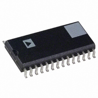
AD9742AR Analog Devices Inc, AD9742AR Datasheet - Page 5

AD9742AR
Manufacturer Part Number
AD9742AR
Description
IC DAC 12BIT 210MSPS 28-SOIC
Manufacturer
Analog Devices Inc
Series
TxDAC®r
Datasheet
1.AD9742ARUZRL7.pdf
(32 pages)
Specifications of AD9742AR
Mounting Type
Surface Mount
Rohs Status
RoHS non-compliant
Settling Time
11ns
Number Of Bits
12
Data Interface
Parallel
Number Of Converters
1
Voltage Supply Source
Analog and Digital
Power Dissipation (max)
145mW
Operating Temperature
-40°C ~ 85°C
Package / Case
28-SOIC (7.5mm Width)
Resolution (bits)
12bit
No. Of Pins
28
Peak Reflow Compatible (260 C)
No
Update Rate
210MSPS
Supply Voltage
3.3V
No. Of Bits
12 Bit
Leaded Process Compatible
No
For Use With
AD9742ACP-PCBZ - BOARD EVAL FOR AD9742ACP
Lead Free Status / RoHS Status
Contains lead / RoHS non-compliant
Available stocks
Company
Part Number
Manufacturer
Quantity
Price
Part Number:
AD9742AR
Manufacturer:
ADI/亚德诺
Quantity:
20 000
Part Number:
AD9742ARU
Manufacturer:
ADI/亚德诺
Quantity:
20 000
Part Number:
AD9742ARUZ
Manufacturer:
ADI/亚德诺
Quantity:
20 000
Part Number:
AD9742ARZ
Manufacturer:
ADI/亚德诺
Quantity:
20 000
Parameter
1
2
3
DIGITAL SPECIFICATIONS
T
Table 3.
Parameter
DIGITAL INPUTS
CLK INPUTS
1
2
Measured single-ended into 50 Ω load.
Output noise is measured with a full-scale output set to 20 mA with no conversion activity. It is a measure of the thermal noise only.
Noise spectral density is the average noise power normalized to a 1 Hz bandwidth, with the DAC converting and producing an output tone.
Includes CLOCK pin on SOIC/TSSOP packages and CLK+ pin on LFCSP package in single-ended clock input mode.
Applicable to CLK+ and CLK− inputs when configured for differential or PECL clock input mode.
MIN
Multitone Power Ratio (8 Tones at 400 kHz Spacing)
Logic 1 Voltage
Logic 0 Voltage
Logic 1 Current
Logic 0 Current
Input Capacitance
Input Setup Time (t
Input Hold Time (t
Latch Pulse Width (t
Input Voltage Range
Common-Mode Voltage
Differential Voltage
f
to T
CLOCK
0 dBFS Output
−6 dBFS Output
−12 dBFS Output
−18 dBFS Output
MAX
= 78 MSPS; f
2
, AVDD = 3.3 V, DVDD = 3.3 V, CLKVDD = 3.3 V, I
1
H
S
)
OUT
)
LPW
)
= 15.0 MHz to 18.2 MHz
DB0–DB11
CLOCK
IOUTA
IOUTB
OR
t
S
Figure 2. Timing Diagram
Rev. B | Page 5 of 32
t
PD
OUTFS
= 20 mA, unless otherwise noted.
0.1%
Min
2.1
−10
−10
2.0
1.5
1.5
0
0.75
0.5
t
t
ST
LPW
t
H
0.1%
Min
Typ
3
0
5
1.5
1.5
Typ
65
67
65
63
Max
0.9
+10
+10
3
2.25
Max
Unit
V
V
µA
µA
pF
ns
ns
ns
V
V
V
Unit
dBc
dBc
dBc
dBc
AD9742


