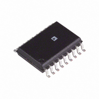
AD7541AKR Analog Devices Inc, AD7541AKR Datasheet - Page 2

AD7541AKR
Manufacturer Part Number
AD7541AKR
Description
IC DAC 12BIT MULT MONO 18-SOIC
Manufacturer
Analog Devices Inc
Datasheet
1.AD7541AKRZ.pdf
(8 pages)
Specifications of AD7541AKR
Rohs Status
RoHS non-compliant
Settling Time
600ns
Number Of Bits
12
Data Interface
Parallel
Number Of Converters
1
Voltage Supply Source
Single Supply
Operating Temperature
0°C ~ 70°C
Mounting Type
Surface Mount
Package / Case
18-SOIC (7.5mm Width)
Power Dissipation (max)
-
Available stocks
Company
Part Number
Manufacturer
Quantity
Price
Company:
Part Number:
AD7541AKRZ
Manufacturer:
Maxim
Quantity:
76
Part Number:
AD7541AKRZ
Manufacturer:
ADI/亚德诺
Quantity:
20 000
Part Number:
AD7541AKRZ-REEL7
Manufacturer:
ADI/亚德诺
Quantity:
20 000
AD7541A–SPECIFICATIONS
Parameter
ACCURACY
REFERENCE INPUT
DIGITAL INPUTS
POWER SUPPLY REJECTION
POWER SUPPLY
AC PERFORMANCE CHARACTERISTICS
These Characteristics are included for Design Guidance only and are not subject to test. V
OUT1 = 0UT2 = GND = 0 V, Output Amp is AD544 except where noted.
Parameter
PROPAGATION DELAY (From Digital Input
DIGITAL TO ANALOG GLITCH
MULTIPLYING FEEDTHROUGH ERROR
OUTPUT CURRENT SETTLING TIME
OUTPUT CAPACITANCE
NOTES
1
2
3
Specifications subject to change without notice.
Temperature range as follows: J, K versions, 0 C to +70 C; A, B versions, –25 C to +85 C; S, T versions, –55 C to +125 C.
Guaranteed by design but not production tested.
To minimize feedthrough in the ceramic package (Suffix D) the user must ground the metal lid.
Resolution
Relative Accuracy
Differential Nonlinearity
Gain Error
Gain Temperature Coefficient
Output Leakage Current
Input Resistance (Pin 17 to GND)
V
V
I
C
V
I
Change to 90% of Final Analog Output)
IMPULSE
(V
C
C
C
C
IN
DD
IH
IL
Gain/ V
DD
IN
OUT1
OUT2
OUT1
OUT2
REF
OUT1 (Pin 1)
OUT2 (Pin 2)
(Input Current)
(Input LOW Voltage)
(Input HIGH Voltage)
Gain/ Temperature
(Input Capacitance)
Range
to OUT1)
(Pin 1)
(Pin 1)
(Pin 2)
(Pin 2)
DD
2
2
3
Version
All
J, A, S
K, B, T
J, A, S
K, B, T
J, A, S
K, B, T
All
J, K
A, B
S, T
J, K
A, B
S, T
All
All
All
All
All
All
All
All
Version
All
All
All
All
All
All
All
All
1
T
+25 C
12
5
7–18
2.4
0.8
8
+5 to +16
2
100
T
+25 C
100
A
1
1/2
1
1/2
6
3
5
5
5
5
5
5
1
0.01
A
1000
1.0
0.6
200
70
70
200
=
=
(V
DD
= +15 V, V
—
—
—
—
200
70
70
200
T
T
12
5
7–18
2.4
0.8
8
+5 to +16
2
500
T
T
–2–
5
10
1
A
MIN,
1
1/2
1
1/2
8
10
10
200
10
200
0.02
A
MIN,
=
=
T
T
REF
MAX
MAX
= +10 V; OUT 1 = OUT 2 = GND = 0 V unless otherwise noted)
1
1
Units
Bits
LSB max
LSB max
LSB max
LSB max
LSB max
LSB max
ppm/ C max
nA max
nA max
nA max
nA max
nA max
nA max
k min/max
V min
V max
pF max
% per % max
V min/V max
mA max
Units
A max
A max
ns typ
pF max
nV-sec typ
mV p-p typ
pF max
pF max
pF max
s typ
DD
= +15 V, V
Digital Inputs = 0 V to V
Test Conditions/Comments
All Grades Guaranteed Monotonic
to 12 Bits, T
Measured Using Internal R
Effect of Leakage Current and Gain TC.
Gain Error Can Be Trimmed to Zero.
Typical Value Is 2 ppm/ C.
All Digital Inputs = 0 V.
All Digital Inputs = V
Typical Input Resistance = 11 k .
Typical Input Resistance Temperature
Coefficient = –300 ppm/ C.
Logic Inputs Are MOS Gates. I
V
Accuracy Is Not Guaranteed Over This Range.
All Digital Inputs V
All Digital Inputs 0 V or V
Test Conditions/Comments
OUT 1 Load = 100 , C
V
V
Measured using Model 50K as output amplifier.
V
To 0.01% of full-scale range.
OUT 1 Load = 100 , C
Digital Inputs = 0 V to V
Digital Inputs
Digital Inputs
1 LSB = 0.024% of Full Scale
1/2 LSB = 0.012% of Full Scale
IN
V
REF
DD
REF
= V
= V
DD
= 0 V
to 0 V.
= 0 V. All digital inputs 0 V to V
= 10 V, 10 kHz sine wave.
IN
IH
IL
= 5%
= +10 V except where noted,
MIN
to T
IL
MAX
DD
or V
.
.
DD
DD
EXT
EXT
IH
DD
FB
.
or V
or V
= 13 pF.
= 13 pF.
.
and Includes
IN
typ (25 C) = 1 nA.
DD
DD
to 0 V.
to 0 V.
DD
REV. B
or


