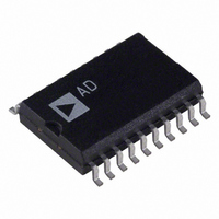
AD7305BRZ Analog Devices Inc, AD7305BRZ Datasheet - Page 8

AD7305BRZ
Manufacturer Part Number
AD7305BRZ
Description
IC DAC 8BIT QUAD 5V R-R 20-SOIC
Manufacturer
Analog Devices Inc
Datasheet
1.AD7304BRZ-REEL.pdf
(20 pages)
Specifications of AD7305BRZ
Data Interface
Parallel
Settling Time
1µs
Number Of Bits
8
Number Of Converters
4
Voltage Supply Source
Dual ±
Power Dissipation (max)
60mW
Operating Temperature
-40°C ~ 85°C
Mounting Type
Surface Mount
Package / Case
20-SOIC (7.5mm Width)
Resolution (bits)
8bit
Sampling Rate
1MSPS
Input Channel Type
Parallel
Supply Voltage Range - Analog
2.7V To 5.5V
Supply Current
6mA
Digital Ic Case Style
SOIC
Lead Free Status / RoHS Status
Lead free / RoHS Compliant
Available stocks
Company
Part Number
Manufacturer
Quantity
Price
Part Number:
AD7305BRZ
Manufacturer:
AD
Quantity:
20 000
Part Number:
AD7305BRZ-REEL
Manufacturer:
ADI/亚德诺
Quantity:
20 000
AD7304/AD7305
PIN CONFIGURATIONS AND FUNCTION DESCRIPTIONS
Table 7. AD7304 Pin Function Descriptions
Pin No.
1
2
3
4
5
6
7
8
9
10
11
12
13
14
15
16
Mnemonic
V
V
V
V
V
GND
LDAC
CLR
CS
CLK
SDI/SHDN
V
V
V
V
V
OUT
OUT
SS
REF
REF
REF
REF
DD
OUT
OUT
A
B
D
C
B
A
D
C
Description
Channel B Rail-to-Rail Buffered DAC Voltage Output. Full-scale set by reference voltage applied to V
Output is open circuit when SHDN is enabled.
Channel A Rail-to-Rail Buffered DAC Voltage Output. Full-scale set by reference voltage applied to V
Output is open circuit when SHDN is enabled.
Negative Power Supply Input. Specified range of operation is 0 V to −5.5 V.
Channel A Reference Input. Establishes V
Channel B Reference Input. Establishes V
Common Analog and Digital Ground.
Load DAC Register Strobe, Active Low. Simultaneously transfers data from all four input registers into the
corresponding DAC registers. Asynchronous active low input. DAC register is transparent when LDAC = 0. See
Table 4 for operation.
Clears All Input and DAC Registers to the Zero Condition. Asynchronous active low input. The serial register is
not effected.
Chip Select, Active Low Input. Disables shift register loading when high. Transfers serial input register data to
the decoded input register when CS returns high. Does not effect LDAC operation.
Clock Input, Positive Edge Clocks Data into Shift Register. Disabled by chip select CS.
Serial Data Input Loads Directly into the Shift Register, MSB First. Hardware shutdown (SHDN) control input,
active when pin is left floating by a three-state logic driver. Does not effect DAC register contents as long as
power is present on V
Channel D Reference Input. Establishes V
Channel C Reference Input. Establishes V
Positive Power Supply Input. Specified range of operation is 2.7 V to 5.5 V.
Channel D Rail-to-Rail Buffered DAC Voltage Output. Full-scale set by reference voltage applied to V
Output is open circuit when SHDN is enabled.
Channel C Rail-to-Rail Buffered DAC Voltage Output. Full-scale set by reference voltage applied to V
Output is open circuit when SHDN is enabled.
DD
.
V
V
V
V
LDAC
OUT
OUT
Figure 8. AD7304 Pin Configuration
REF
REF
GND
CLR
V
SS
B
A
A
B
1
2
3
4
5
6
7
8
Rev. C | Page 8 of 20
(Not to Scale)
AD7304
TOP VIEW
OUT
OUT
OUT
OUT
B full-scale voltage. Specified range of operation is V
A full-scale voltage. Specified range of operation is V
C full-scale voltage. Specified range of operation is V
D full-scale voltage. Specified range of operation is V
16
15
14
13
12
11
10
9
V
V
V
V
V
SDI/SHDN
CLK
CS
OUT
OUT
DD
REF
REF
C
D
C
D
SS
SS
SS
SS
< V
< V
V
< V
REF
REF
REF
REF
REF
REF
REF
REF
C < V
B pin.
A pin.
C pin.
D pin.
B < V
A < V
D < V
DD
DD
DD
.
DD
.
.
.


