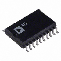
AD7948BR Analog Devices Inc, AD7948BR Datasheet - Page 9

AD7948BR
Manufacturer Part Number
AD7948BR
Description
IC DAC 12BIT MULTIPLYING 20-SOIC
Manufacturer
Analog Devices Inc
Datasheet
1.AD7943BNZ.pdf
(16 pages)
Specifications of AD7948BR
Rohs Status
RoHS non-compliant
Settling Time
600ns
Number Of Bits
12
Data Interface
Parallel
Number Of Converters
1
Voltage Supply Source
Single Supply
Power Dissipation (max)
25µW
Operating Temperature
-40°C ~ 85°C
Mounting Type
Surface Mount
Package / Case
20-SOIC (7.5mm Width)
Available stocks
Company
Part Number
Manufacturer
Quantity
Price
Part Number:
AD7948BR
Manufacturer:
ADI/亚德诺
Quantity:
20 000
Part Number:
AD7948BRSZ
Manufacturer:
ADI/亚德诺
Quantity:
20 000
Part Number:
AD7948BRSZ-REEL
Manufacturer:
ADI/亚德诺
Quantity:
20 000
Part Number:
AD7948BRZ
Manufacturer:
ADI/亚德诺
Quantity:
20 000
REV. B
Pin Mnemonic
I
I
AGND
STB1
LD1, LD2
SRI
STB2
STB3
STB4
DGND
CLR
V
V
R
Pin Mnemonic
I
AGND
DGND
DB11–DB0
CS
WR
V
V
R
OUT1
OUT2
OUT1
DD
REF
FB
DD
REF
FB
This pin connects to the back gates of the current steering switches. In normal operation, it should be connected
This is the Strobe 1 input. Data is clocked into the input shift register on the rising edge of this signal. STB3
Serial Data Input. Data on this line will be clocked into the input shift register on one of the Strobe inputs,
This is the Strobe 2 input. Data is clocked into the input shift register on the rising edge of this signal.
This is the Strobe 4 input. Data is clocked into the input shift register on the rising edge of this signal. STB3
Digital Ground.
This pin connects to the back gates of the current steering switches. The DAC I
Digital Ground.
Digital Data Inputs.
Description
DAC current output terminal 1.
DAC current output terminal 2. This should be connected to the AGND pin.
to the signal ground of the system. In biased single-supply operation it may be biased to some voltage between
0 V and the 1.23 V. See Figure 11 for more details.
Active low inputs. When both of these are low, the DAC register is updated and the output will change to
reflect this.
when they are enabled.
STB3 must be high. STB1, STB4 must be low.
This is the Strobe 3 input. Data is clocked into the input shift register on the falling edge of this signal. STB1,
STB2, STB4, must be low.
must be high. STB1, STB2 must be low.
Asynchronous CLR input. When this input is taken low, all 0s are loaded to the DAC latch.
Power supply input. This is nominally +5 V for Normal Mode Operation and +3.3 V to +5 V for Biased
Mode Operation.
DAC reference input.
DAC feedback resistor pin.
Description
DAC current output terminal 1.
internally to this point.
Active Low, Chip Select Input.
Active Low, Write Input.
Power supply input. This is nominally +5 V for Normal Mode Operation and +3.3 V to +5 V for Biased Mode
Operation.
DAC reference input.
DAC feedback resistor pin.
must be high. STB2, STB4 must be low.
AD7943 PIN FUNCTION DESCRIPTIONS
AD7945 PIN FUNCTION DESCRIPTIONS
–9–
AD7943/AD7945/AD7948
OUT2
terminal is also connected


