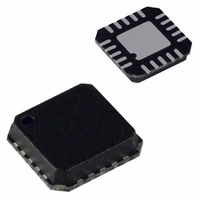
AD5424YCPZ-REEL7 Analog Devices Inc, AD5424YCPZ-REEL7 Datasheet - Page 7

AD5424YCPZ-REEL7
Manufacturer Part Number
AD5424YCPZ-REEL7
Description
IC DAC 8BIT MULTIPLYING 20-LFCSP
Manufacturer
Analog Devices Inc
Datasheet
1.AD5445YRUZ.pdf
(32 pages)
Specifications of AD5424YCPZ-REEL7
Settling Time
30ns
Number Of Bits
8
Data Interface
Parallel
Number Of Converters
1
Voltage Supply Source
Single Supply
Power Dissipation (max)
25µW
Operating Temperature
-40°C ~ 125°C
Mounting Type
Surface Mount
Package / Case
20-LFCSP
For Use With
EVAL-AD5424EBZ - BOARD EVALUATION FOR AD5424
Lead Free Status / RoHS Status
Lead free / RoHS Compliant
PIN CONFIGURATION AND FUNCTION DESCRIPTIONS
Table 4. AD5424 Pin Function Descriptions
TSSOP
1
2
3
4–11
12
13
14
15
16
Pin No.
LFCSP
19
20
1
2–9
10–13
14
15
16
17
18
Figure 3. AD5424 Pin Configuration (TSSOP)
I
I
OUT
OUT
GND
DB7
DB6
DB5
DB4
DB3
1
2
Mnemonic
I
I
GND
DB7–DB0
NC
CS
R/W
V
V
R
1
2
3
4
5
6
7
8
OUT
OUT
DD
REF
FB
1
2
(Not to Scale)
AD5424
Description
DAC Current Output.
DAC Analog Ground. This pin should normally be tied to the analog ground of the system.
Ground.
Parallel Data Bits 7 to 0.
No Internal Connection.
Chip Select Input. Active low. Used in conjunction with R/W to load parallel data to the input latch or to
read data from the DAC register. Rising edge of CS loads data.
Read/Write. When low, use in conjunction with CS to load parallel data. When high, use with CS to read
back contents of DAC register.
Positive Power Supply Input. These parts can be operated from a supply of 2.5 V to 5.5 V.
DAC Reference Voltage Input Terminal.
DAC Feedback Resistor Pin. Establish voltage output for the DAC by connecting to external amplifier
output.
16
15
14
13
12
11
10
9
R
V
V
R/W
CS
DB0 (LSB)
DB1
DB2
REF
DD
FB
Rev. B | Page 7 of 32
Figure 4. AD5424 Pin Configuration (LFCSP)
GND
DB7
DB6
DB5
DB4
1
2
3
4
5
NC = NO CONNECT
AD5424/AD5433/AD5445
20 19 18 17 16
6 7 8 9 10
AD5424
TOP VIEW
PIN 1
INDICATOR
15
14
13
12
11
R/W
CS
NC
NC
NC


