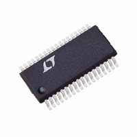
LTC1821-1ACGW#PBF Linear Technology, LTC1821-1ACGW#PBF Datasheet - Page 8

LTC1821-1ACGW#PBF
Manufacturer Part Number
LTC1821-1ACGW#PBF
Description
IC D/A CONV 16BIT PRECISE 36SSOP
Manufacturer
Linear Technology
Datasheet
1.LTC1821-1BCGWPBF.pdf
(16 pages)
Specifications of LTC1821-1ACGW#PBF
Settling Time
2µs
Number Of Bits
16
Data Interface
Parallel
Number Of Converters
1
Voltage Supply Source
Single Supply
Operating Temperature
0°C ~ 70°C
Mounting Type
Surface Mount
Package / Case
36-SSOP
Lead Free Status / RoHS Status
Lead free / RoHS Compliant
Power Dissipation (max)
-
Available stocks
Company
Part Number
Manufacturer
Quantity
Price
Table 1
BLOCK DIAGRA
LTC1821
TRUTH TABLE
8
CONTROL INPUTS
CLR
0
1
1
1
1
1
R
REF
COM
V
WR
R1 10
LD
CC
23
24
WR
8
9
2
X
0
1
0
1
12k
12k
LD
X
0
1
1
0
48k
REGISTER OPERATION
Reset Input and DAC Register to All 0s for LTC1821 and Midscale for LTC1821-1 (Asynchronous Operation)
Write Input Register with All 16 Data Bits
Load DAC Register with the Contents of the Input Register
Input and DAC Register Are Transparent
CLK = LD and WR Tied Together. The 16 Data Bits Are Written Into the Input Register on the Falling Edge of the CLK and Then
Loaded Into the DAC Register on the Rising Edge of the CLK
No Register Operation
48k
W
48k
LOAD
DECODER
(MSB)
D15
48k
D15
WR
25
D14
48k
26
D14
48k
D13
DAC REGISTER
• • • •
INPUT REGISTER
48k
D12
96k
36
D4
48k
D11
D3
3
96k
D2
• • •
4
48k
D1
5
(LSB)
D0
96k
RST
RST
D0
6
96k
*CONNECTED INTERNALLY.
DO NOT CONNECT EXTERNAL
CIRCUITRY TO THESE PINS
12k
12k
–
+
1821 BD
11
13
20
16
17
19
12
14
15
18
21
22
7
1
R
R
I
V
V
V
AGNDS
AGNDF
CLR
DNC*
DNC*
DNC*
NC
DGND
OUT
FB
OFS
+
OUT
–


