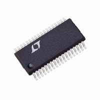
LTC1821-1ACGW Linear Technology, LTC1821-1ACGW Datasheet

LTC1821-1ACGW
Specifications of LTC1821-1ACGW
Available stocks
Related parts for LTC1821-1ACGW
LTC1821-1ACGW Summary of contents
Page 1
... Precise 16-bit bipolar 10V outputs are achieved with on-chip 4-quadrant multiplication resistors. The LTC1821 is available in a 36-lead SSOP package and is specified over the industrial temperature range. The device includes an internal deglitcher circuit that reduces the glitch impulse to less than 2nV• ...
Page 2
... MIN MAX MIN MAX 10 – 4.5V to 16. INFORMATION ORDER PART TOP VIEW NUMBER LTC1821ACGW LTC1821BCGW 31 D9 LTC1821-1ACGW 30 D10 29 D11 LTC1821-1BCGW 28 D12 LTC1821AIGW 27 D13 26 D14 LTC1821BIGW 25 D15 LTC1821-1AIGW 24 WR LTC1821-1BIGW DNC* – DNC* GW PACKAGE = 125 *DO NOT CONNECT = T A MIN LTC1821B/-1B LTC1821A/-1A MIN ...
Page 3
... L + – 2k 5V – – 15V –15V, 5mA Load + – 0V 15V –15V OUT + – 2k 15V –15V L + – 2k 5V –5V L (Note Digital Inputs = 15V 5V LTC1821 = MIN MAX MIN TYP MAX UNITS 4 nV•s 2 nV• P-P 600 kHz 13 nV nV/ Hz 0.45 V RMS 1 ...
Page 4
... LTC1821 ELECTRICAL CHARACTERISTICS Note 1: Absolute Maximum Ratings are those values beyond which the life of a device may be impaired. Note 2: 1LSB = 0.0015% of full scale = 15.3ppm of full scale. Note 3: Using internal feedback resistor. Note 4: Guaranteed by design, not subject to test. Note 5: I with DAC register loaded to all 0s. ...
Page 5
... V = 10V REF – 0 2.5V REF – 0.4 – 0.6 – 0.8 –1 SUPPLY VOLTAGE (V) LTC1821 Differential Nonlinearity (DNL) 1.0 0.8 0.6 0.4 0.2 0 – 0.2 – 0.4 – 0.6 – 0.8 –1.0 65535 0 16384 32768 DIGITAL INPUT CODE 1821 G08 Differential Nonlinearity vs Reference Voltage in Unipolar Mode 1 ...
Page 6
... TO ZERO SCALE D14 D14 D14 D15 ON – 100 10M 10 100 1k 10k 100k FREQUENCY (Hz) 1821 G19 *DAC ZERO VOLTAGE OUTPUT LIMITED BY BIPOLAR ZERO ERROR TO – 96dB TYPICAL (–78dB MAX, A GRADE) V REF LT1468 – 2 12pF 12pF OUT 13 LTC1821 10M 1821 G20 15pF V OUT ...
Page 7
... CLR (Pin 7): Digital Clear Control Function for the DAC. When CLR is taken to a logic low, it sets the DAC output and all internal registers to: zero code for the LTC1821 and midscale code for the LTC1821-1. REF (Pin 8): Reference Input and 4-Quadrant Resistor R2. ...
Page 8
... LTC1821 TRUTH TABLE Table 1 CONTROL INPUTS CLR WR LD REGISTER OPERATION Reset Input and DAC Register to All 0s for LTC1821 and Midscale for LTC1821-1 (Asynchronous Operation Write Input Register with All 16 Data Bits Load DAC Register with the Contents of the Input Register Input and DAC Register Are Transparent 1 CLK = LD and WR Tied Together ...
Page 9
... LTC1821 can go as low as 4.5V and 4.5V. In this case for a 2.5V or – 2.5V reference, the output range – 2.5V 2.5V and 2.5V. The LTC1821 has three additional precision resistors on chip for bipolar operation. Refer to the block diagram regarding the fol- lowing description ...
Page 10
... DAC registers in a master slave or edge-triggered configuration. This mode of operation occurs when WR and LD are tied together. The asynchronous clear pin resets the LTC1821 to zero scale and the LTC1821-1 to midscale. CLR resets both the input and DAC registers. These devices also have a power-on reset. Table 1 shows the truth table for the LTC1821 ...
Page 11
... U U APPLICATIONS INFORMATION Bipolar Mode (4-Quadrant Multiplying – V OUT The LTC1821 contains on chip all the 4-quadrant resistors necessary for bipolar operation. 4-quadrant multiplying V REF COM DATA INPUTS LTC1821 CLR Figure 2. Bipolar Operation (4-Quadrant Multiplication operation can be achieved with a minimum of external ...
Page 12
... Because of the extremely high accuracy of the 16-bit LTC1821, careful thought should be given to the selection of a precision voltage reference. As shown in the section describing the basic operation of the LTC1821, the output voltage of the DAC circuit is directly affected by the voltage reference; thus, any voltage reference error will appear as a DAC output voltage error ...
Page 13
... R R2 OFS FB 16-BIT DAC CLR DNC* DNC* DNC* NC DGND AGNDF *DO NOT CONNECT ERA82.004 ALTERNATE AMPLIFIER FOR OPTIMUM SETTLING TIME PERFORMANCE 16 AGNDS AGNDF 17 6 LT1468 ERA82.004 LTC1821 22pF 14 I OUT + 15 V 15V 0.1 F – OUT 0V TO –10V V OUT + – –15V AGNDS 16 0.1 F ...
Page 14
... INPUTS CLR 14 14 LTC203AC 3 0 0.1 F LT1468 2 – 0.1 F – V 15pF REF R COM CC OFS OFS R2 FB 16-BIT DAC LTC1821 LD CLR DNC* DNC* DNC* NC DGND 22pF OUT + V 15 – OUT + – AGNDF AGNDS *DO NOT CONNECT 1821 TA03 15V 0 OUT –15V 0.1 F ...
Page 15
... TYP 0.800 (0.0315) BSC ** DIMENSION DOES NOT INCLUDE INTERLEAD FLASH. INTERLEAD FLASH SHALL NOT EXCEED 0.254mm (0.010") PER SIDE LTC1821 15.290 – 15.544* (0.602 – 0.612) 10.160 – 10.414 (0.400 – 0.410) 2.286 – 2.387 (0.090 – 0.094) 0.127 – 0.305 0.304 – ...
Page 16
... LTC1821 RELATED PARTS PART NUMBER DESCRIPTION ADCs LTC1417 Low Power 400ksps, 14-Bit ADC LTC1418 14-Bit, 200ksps, Single 5V ADC LTC1604/LTC1608 16-Bit, 333ksps/500ksps, 5V ADC LTC1605/LTC1606 16-Bit, 100ksps/250ksps, Single 5V ADC LTC1609 16-Bit, 200ksps, Single 5V ADC LTC2400 24-Bit, Micropower LTC2410 24-Bit, Fully Differential, No Latency DACs ...


