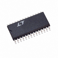
LTC1458CSW Linear Technology, LTC1458CSW Datasheet - Page 8

LTC1458CSW
Manufacturer Part Number
LTC1458CSW
Description
IC D/A CONV 12BIT R-R QUAD28SOIC
Manufacturer
Linear Technology
Datasheet
1.LTC1458CSWPBF.pdf
(12 pages)
Specifications of LTC1458CSW
Settling Time
14µs
Number Of Bits
12
Data Interface
Serial
Number Of Converters
4
Voltage Supply Source
Single Supply
Power Dissipation (max)
5.5mW
Operating Temperature
0°C ~ 70°C
Mounting Type
Surface Mount
Package / Case
28-SOIC (7.5mm Width)
Lead Free Status / RoHS Status
Contains lead / RoHS non-compliant
Available stocks
Company
Part Number
Manufacturer
Quantity
Price
Company:
Part Number:
LTC1458CSW
Manufacturer:
MAX
Quantity:
13
Company:
Part Number:
LTC1458CSW#PBF
Manufacturer:
LTC
Quantity:
249
DEFI ITIO S
Differential Nonlinearity (DNL): DNL is the difference
between the measured change and the ideal 1LSB change
between any two adjacent codes. The DNL error between
any two codes is calculated as follows:
OPERATIO
Serial Interface
The data on the D
on the rising edge of the clock. Data is loaded as one 48-bit
word, DAC A first, then DAC B, DAC C and DAC D. The MSB
is loaded first for each DAC. The DAC registers load the
data from the shift register when CS/LD is pulled high. The
CLK is disabled internally when CS/LD is high. Note: CLK
must be low before CS/LD is pulled low to avoid an extra
internal clock pulse.
The buffered output of the 48-bit shift register is available
on the D
Multiple LTC1458/LTC1458Ls may be daisy-chained to-
gether by connecting the D
chip, while the CLK and CS/LD signals remain common to
all chips in the daisy-chain. The serial data is clocked to all
of the chips, then the CS/LD signal is pulled high to update
all of them simultaneously.
LTC1458/LTC1458L
8
DNL
V
OUT
U
OUT
= ( V
= The measured voltage difference between
pin which swings from ground to V
two adjacent codes
U
OUT
U
IN
input is loaded into the shift register
– LSB)/LSB
OUT
pin to the D
IN
pin of the next
CC
.
Reference
The LTC1458L has an internal reference of 1.22V with a full
scale of 2.5V (gain of 2 configuration). The LTC1458
includes an internal 2.048V reference, making 1LSB equal
to 1mV (gain of 2 configuration). When the buffer gain is
2, the external reference must be less than V
capable of driving the 15k minimum DAC resistor ladder.
The external reference must always be less than
V
density at 1kHz is 300nV/ Hz.
Voltage Output
The rail-to-rail buffered output of the LTC1458 family can
source or sink 5mA when operating with a 5V supply over
the entire operating temperature range while pulling to
within 300mV of the positive supply voltage or ground.
The output swings to within a few millivolts of either
supply rail when unloaded and has an equivalent output
resistance of 40 when driving a load to the rails. The
output can drive 1000pF without going into oscillation.
The output voltage noise spectral density at 1kHz is
600nV/ Hz.
Digital Feedthrough: The glitch that appears at the analog
output caused by AC coupling from the digital inputs when
they change state. The area of the glitch is specified in
(nV)(sec).
CC
– 1.5V. The reference output voltage noise spectral
CC
/2 and be


