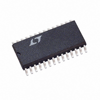
LTC1458CSW Linear Technology, LTC1458CSW Datasheet - Page 7

LTC1458CSW
Manufacturer Part Number
LTC1458CSW
Description
IC D/A CONV 12BIT R-R QUAD28SOIC
Manufacturer
Linear Technology
Datasheet
1.LTC1458CSWPBF.pdf
(12 pages)
Specifications of LTC1458CSW
Settling Time
14µs
Number Of Bits
12
Data Interface
Serial
Number Of Converters
4
Voltage Supply Source
Single Supply
Power Dissipation (max)
5.5mW
Operating Temperature
0°C ~ 70°C
Mounting Type
Surface Mount
Package / Case
28-SOIC (7.5mm Width)
Lead Free Status / RoHS Status
Contains lead / RoHS non-compliant
Available stocks
Company
Part Number
Manufacturer
Quantity
Price
Company:
Part Number:
LTC1458CSW
Manufacturer:
MAX
Quantity:
13
Company:
Part Number:
LTC1458CSW#PBF
Manufacturer:
LTC
Quantity:
249
DEFI ITIO S
TI I G DIAGRA
Resolution (n): Resolution is defined as the number of
digital input bits, n. It defines the number of DAC output
states (2
does not imply linearity.
Full-Scale Voltage (V
when all bits are set to 1.
Voltage Offset Error (V
output when the DAC is loaded with all zeros. The output
amplifier can have a true negative offset, but because the
part is operated from a single supply, the output cannot go
below zero. If the offset is negative, the output will remain
near 0V resulting in the transfer curve shown in Figure 1.
CS/LD
D
CLK
OUT
D
W
IN
U
U
NEGATIVE
PREVIOUS WORD
n
) that divide the full-scale range. The resolution
OFFSET
VOLTAGE
OUTPUT
B0 D
Figure 1. Effect of Negative Offset
U
0V
PREVIOUS WORD
t
9
B11 A
FS
OS
): This is the output of the DAC
): The theoretical voltage at the
DAC CODE
W
B11 A
MSB
PREVIOUS WORD
B10 A
t
4
1458 F01
PREVIOUS WORD
B0 B
t
B0 B
8
LSB
t
3
The offset of the part is measured at the code that corre-
sponds to the maximum offset specification:
Least Significant Bit (LSB): One LSB is the ideal voltage
difference between two successive codes.
Nominal LSBs:
Integral Nonlinearity (INL): End-point INL is the maxi-
mum deviation from a straight line passing through the
end-points of the DAC transfer curve. Because the part
operates from a single supply and the output cannot go
below zero, the linearity is measured between full scale
and the code corresponding to the maximum offset
specification. The INL error at a given input code is
calculated as follows:
PREVIOUS WORD
V
LSB = (V
LTC1458
LTC1458L
INL
V
OS
OUT
B11 C
= V
t
1
= [V
= The output voltage of the DAC measured at
OUT
B11 C
MSB
FS
the given input code
t
– V
OUT
2
– [(Code)(V
LSB = 4.095V/4095 = 1mV
LSB = 2.5V/4095 = 0.610mV
OS
– V
)/(2
OS
LTC1458/LTC1458L
n
– (V
– 1) = (V
FS
PREVIOUS WORD
)/(2
FS
– V
B0 D
n
– 1)]
FS
OS
B0 D
LSB
– V
t
)(code/4095)]/LSB
6
OS
)/4095
t
5
CURRENT WORD
B11 A
t
7
7
1458 TD


