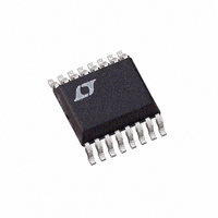
LTC1660IGN Linear Technology, LTC1660IGN Datasheet - Page 7

LTC1660IGN
Manufacturer Part Number
LTC1660IGN
Description
IC D/A CONV 10BIT OCTAL 16-SSOP
Manufacturer
Linear Technology
Datasheet
1.LTC1665CGNPBF.pdf
(16 pages)
Specifications of LTC1660IGN
Settling Time
30µs
Number Of Bits
10
Data Interface
Serial
Number Of Converters
8
Voltage Supply Source
Single Supply
Power Dissipation (max)
1mW
Operating Temperature
-40°C ~ 85°C
Mounting Type
Surface Mount
Package / Case
16-SSOP
Lead Free Status / RoHS Status
Contains lead / RoHS non-compliant
Available stocks
Company
Part Number
Manufacturer
Quantity
Price
Company:
Part Number:
LTC1660IGN
Manufacturer:
LT
Quantity:
10 000
Part Number:
LTC1660IGN
Manufacturer:
LINEAR/凌特
Quantity:
20 000
Part Number:
LTC1660IGN#PBF
Manufacturer:
LINEAR/凌特
Quantity:
20 000
Part Number:
LTC1660IGN#TRPBF
Manufacturer:
LINEAR/凌特
Quantity:
20 000
PIN
GND (Pin 1): System Ground.
V
Voltage Outputs. The output range is
REF (Pin 6): Reference Voltage Input. 0V V
CS/LD (Pin 7): Serial Interface Chip Select/Load Input.
When CS/LD is low, SCK is enabled for shifting data on D
into the register. When CS/LD is pulled high, SCK is
disabled and data is loaded from the shift register into the
specified DAC register(s), updating the analog output(s).
CMOS and TTL compatible.
BLOCK DIAGRA
OUT A
U
0
0
to
to
FUNCTIONS
to V
256
1023
1024
255
U
OUT H
V
REF
V
REF
(Pins 2-5 and 12-15): DAC Analog
for the LTC
U
for the LTC
V
V
V
V
W
CS/LD
(LTC1665/LTC1660)
OUT D
OUT A
OUT B
OUT C
GND
SCK
REF
1665
1
2
3
4
5
6
7
8
1660
DAC D
DAC A
DAC B
DAC C
REF
CONTROL
LOGIC
V
CC
SHIFT REGISTER
IN
.
SCK (Pin 8): Serial Interface Clock Input. CMOS and TTL
compatible.
D
is shifted into the 16-bit register on the rising edge of SCK.
CMOS and TTL compatible.
D
on D
May be tied to D
chain operaton. CMOS and TTL compatible.
CLR (Pin 11): Asynchronous Clear Input. All internal shift
and DAC registers are cleared to zero at the falling edge of
the CLR signal, forcing the analog outputs to zero scale.
CMOS and TTL compatible.
V
CC
IN
OUT
ADDRESS
DECODER
(Pin 9): Serial Interface Data Input. Data on the D
(Pin 16): Supply Voltage Input. 2.7V V
OUT
(Pin 10): Serial Interface Data Output. Data appears
DAC H
DAC G
DAC F
DAC E
16 positive SCK edges after being applied to D
IN
of another LTC1665/LTC1660 for daisy-
11
10
16
15
14
13
12
9
LTC1665/LTC1660
1665/60 BD
V
V
V
V
V
CLR
D
D
CC
OUT H
OUT G
OUT F
OUT E
OUT
IN
CC
5.5V.
IN
7
pin
IN
.


