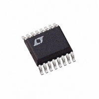
LTC1660IGN Linear Technology, LTC1660IGN Datasheet

LTC1660IGN
Specifications of LTC1660IGN
Available stocks
Related parts for LTC1660IGN
LTC1660IGN Summary of contents
Page 1
... LTC1665 and LTC1660 ideal for battery-powered applications, while their ease of use, high performance and wide supply range make them excellent choices as general purpose converters. , LTC and LT are registered trademarks of Linear Technology Corporation. LTC1665 Differential Nonlinearity (DNL) 0.5 0.4 ...
Page 2
... TOP VIEW 16 V LTC1665CGN LTC1665CN OUT LTC1665IGN OUT LTC1665IN OUT OUT E LTC1660CGN 11 CLR LTC1660CN 10 D OUT LTC1660IGN LTC1660IN N PACKAGE GN PART MARKING 16-LEAD PDIP = 150 C/W (GN) JA 1665 = 100 C/W (N) JA 1665I LTC1665 LTC1660 TYP MAX MIN TYP MAX 0.1 0.5 0.2 ...
Page 3
ELECTRICAL C HARA TERISTICS C The denotes specifications which apply over the full operating temperature range, otherwise specifications are 2.7V to 5.5V REF SYMBOL PARAMETER CONDITIONS DC Performance Short-Circuit Current ...
Page 4
LTC1665/LTC1660 CHARACTERISTICS range, otherwise specifications are SYMBOL PARAMETER t LSB SCK High to CS/LD High 6 t CS/LD Low to SCK High Propagation Delay 8 OUT t SCK Low ...
Page 5
W U TYPICAL PERFOR A CE CHARACTERISTICS Minimum Supply Headroom vs Load Current (Output Sourcing) 1400 V = 4.096V REF V < 1LSB OUT 1200 CODE = 255 (LTC1665) CODE = 1023 (LTC1660) 1000 800 600 400 200 0 0 ...
Page 6
LTC1665/LTC1660 W U TYPICAL PERFOR A CE CHARACTERISTICS Load Regulation vs Output Current 0.5 CC REF CODE = 128 0.25 0 –0.25 SOURCE –0.5 –2 – OUT W U TYPICAL PERFOR A CE ...
Page 7
PIN FUNCTIONS (LTC1665/LTC1660) GND (Pin 1): System Ground (Pins 2-5 and 12-15): DAC Analog OUT A OUT H Voltage Outputs. The output range is 255 for the LTC 1665 REF 256 ...
Page 8
LTC1665/LTC1660 DIAGRA SCK CS/ OUT U OPERATIO Transfer Function The transfer function for the LTC OUT IDEAL ( ) REF 256 ...
Page 9
U OPERATIO SCK ADDRESS/CONTROL (ENABLE CLK) CS/ OUT SCK ADDRESS/CONTROL (ENABLE CLK) CS/ OUT Table 1a. LTC1665 Input ...
Page 10
LTC1665/LTC1660 U OPERATIO Table 2. DAC Address/Control Functions ADDRESS/CONTROL DAC STATUS Change Load DAC Load DAC Load ...
Page 11
U OPERATIO OUTPUT VOLTAGE 0V NEGATIVE INPUT CODE OFFSET (b) Figure 3. Effects of Rail-to-Rail Operation On a DAC Transfer Curve. (a) Overall Transfer Function (b) Effect of Negative Offset for Codes Near Zero Scale (c) Effect of Positive Full-Scale ...
Page 12
LTC1665/LTC1660 U TYPICAL APPLICATIONS A Low Power Quad Trim Circuit with Coarse/Fine Adjustment 3. 0 GND 2 1 – 1 U2A R1 ® LT 1491 COARSE V V OUT1 3 OUT 0.1 ...
Page 13
U TYPICAL APPLICATIONS An 8-Channel Bipolar Output Voltage Circuit Configuration GND 4 2 – U2A OUT A LT1491 OUT – ...
Page 14
LTC1665/LTC1660 PACKAGE DESCRIPTION 0.007 – 0.0098 (0.178 – 0.249) 0.016 – 0.050 (0.406 – 1.270) * DIMENSION DOES NOT INCLUDE MOLD FLASH. MOLD FLASH SHALL NOT EXCEED 0.006" (0.152mm) PER SIDE ** DIMENSION DOES NOT INCLUDE INTERLEAD FLASH. INTERLEAD FLASH ...
Page 15
... MOLD FLASH OR PROTRUSIONS SHALL NOT EXCEED 0.010 INCH (0.254mm) Information furnished by Linear Technology Corporation is believed to be accurate and reliable. However, no responsibility is assumed for its use. Linear Technology Corporation makes no represen- tation that the interconnection of its circuits as described herein will not infringe on existing patent rights. ...
Page 16
... External Reference Can Be Tied 4.5V to 5.5V 4.095V CC OUT = 2.7V to 5.5V 2.5V CC OUT = 4.5V to 5.5V 4.095V CC OUT = 2.7V to 5.5V 2.5V CC OUT = 4.5V to 5.5V, 4-Quadrant Multiplication CC DAC. Output Swings from OUT CC 166560f LT/TP 0999 4K • PRINTED IN THE USA LINEAR TECHNOLOGY CORPORATION 1999 CC ...


