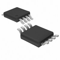
LTC2602CMS8#TR Linear Technology, LTC2602CMS8#TR Datasheet - Page 3

LTC2602CMS8#TR
Manufacturer Part Number
LTC2602CMS8#TR
Description
IC DAC 16BIT DUAL R-R VOUT 8MSOP
Manufacturer
Linear Technology
Datasheet
1.LTC2622IMS8PBF.pdf
(16 pages)
Specifications of LTC2602CMS8#TR
Settling Time
10µs
Number Of Bits
16
Data Interface
Serial
Number Of Converters
2
Voltage Supply Source
Single Supply
Power Dissipation (max)
6.5mW
Operating Temperature
0°C ~ 70°C
Mounting Type
Surface Mount
Package / Case
8-MSOP, Micro8™, 8-uMAX, 8-uSOP,
Lead Free Status / RoHS Status
Contains lead / RoHS non-compliant
Available stocks
Company
Part Number
Manufacturer
Quantity
Price
SYMBOL PARAMETER
AC Performance
t
e
temperature range, otherwise specifications are at T
SYMBOL
PSRR
R
I
Reference Input
I
Power Supply
V
I
Digital I/O
V
V
I
C
ELECTRICAL C
s
SC
REF
CC
LK
n
CC
IH
IL
IN
OUT
Settling Time (Note 8)
Settling Time for
1LSB Step (Note 9)
Voltage Output Slew Rate
Capacitive Load Driving
Glitch Impulse
Multiplying Bandwidth
Output Voltage Noise
Density
Output Voltage Noise
PARAMETER
Power Supply Rejection Ratio
DC Output Impedance
DC Crosstalk (Note 4)
Short-Circuit Output Current
Input Voltage Range
Resistance
Capacitance
Reference Current, Power Down Mode All DACs Powered Down
Positive Supply Voltage
Supply Current
Digital Input High Voltage
Digital Input Low Voltage
Digital Input Leakage
Digital Input Capacitance
HARA TERISTICS
CONDITIONS
±0.024% (±1LSB at 12 Bits)
±0.006% (±1LSB at 14 Bits)
±0.0015% (±1LSB at 16 Bits)
±0.024% (±1LSB at 12 Bits)
±0.006% (±1LSB at 14 Bits)
±0.0015% (±1LSB at 16 Bits)
At Midscale Transition
At f = 1kHz
At f = 10kHz
0.1Hz to 10Hz
C
CONDITIONS
V
V
V
Due to Full Scale Output Change (Note 5)
Due to Load Current Change
Due to Powering Down (per Channel)
V
Code: Zero Scale; Forcing Output to V
Code: Full Scale; Forcing Output to GND
V
Code: Zero Scale; Forcing Output to V
Code: Full Scale; Forcing Output to GND
Normal Mode
For Specified Performance
V
V
All DACs Powered Down (Note 3) V
All DACs Powered Down (Note 3) V
V
V
V
V
V
V
(Note 6)
CC
REF
REF
CC
CC
CC
CC
CC
CC
CC
CC
CC
IN
= GND to V
= 5V ±10%
= 5.5V, V
= 2.5V, V
= 5V (Note 3)
= 3V (Note 3)
= 2.5V to 5.5V
= 2.5V to 3.6V
= 4.5V to 5.5V
= 2.7V to 5.5V
= 2.5V to 5.5V
= V
= V
A
CC
CC
= 25°C. V
= 5V, Midscale; –15mA ≤ I
= 2.5V, Midscale; –7.5mA ≤ I
REF
REF
The
CC
= 5.5V
= 2.5V
●
CC
denotes specifications which apply over the full operating
= 2.5V to 5.5V, V
MIN
LTC2622
1000
0.80
TYP MAX
180
120
100
2.7
12
15
7
LTC2602/LTC2612/LTC2622
CC
CC
CC
CC
OUT
= 5V
= 3V
OUT
≤ 15mA
REF
≤ 7.5mA
≤ V
MIN
CC
LTC2612
, V
1000
0.80
TYP MAX
180
120
100
2.7
4.8
●
●
●
●
●
●
●
●
●
●
●
●
●
●
●
●
●
●
●
●
●
12
15
OUT
7
9
unloaded, unless otherwise noted.
LTC2602/LTC2612/LTC2622
MIN
7.5
7.5
2.5
2.4
2.0
15
15
44
0
MIN
0.001
0.05
0.05
0.35
0.10
TYP
–80
±30
±16
0.7
0.6
20
28
±4
34
38
64
23
LTC2602
1000
0.80
TYP MAX
180
120
100
2.7
4.8
5.2
10
12
15
7
9
MAX
0.15
0.15
V
5.5
1.3
0.8
0.6
0.5
±1
60
60
50
50
80
1
1
1
1
8
CC
nV/√Hz
nV/√Hz
µV/mA
UNITS
UNITS
nV • s
µV
2602fa
3
V/µs
kHz
mA
mA
mA
mA
mA
mA
P-P
kΩ
dB
µV
µV
µA
µA
µA
µA
µs
µs
µs
µs
µs
µs
pF
pF
pF
Ω
Ω
V
V
V
V
V
V
V


