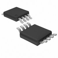
LTC2602CMS8#TR Linear Technology, LTC2602CMS8#TR Datasheet - Page 11

LTC2602CMS8#TR
Manufacturer Part Number
LTC2602CMS8#TR
Description
IC DAC 16BIT DUAL R-R VOUT 8MSOP
Manufacturer
Linear Technology
Datasheet
1.LTC2622IMS8PBF.pdf
(16 pages)
Specifications of LTC2602CMS8#TR
Settling Time
10µs
Number Of Bits
16
Data Interface
Serial
Number Of Converters
2
Voltage Supply Source
Single Supply
Power Dissipation (max)
6.5mW
Operating Temperature
0°C ~ 70°C
Mounting Type
Surface Mount
Package / Case
8-MSOP, Micro8™, 8-uMAX, 8-uSOP,
Lead Free Status / RoHS Status
Contains lead / RoHS non-compliant
Available stocks
Company
Part Number
Manufacturer
Quantity
Price
OPERATIO
INPUT WORD (LTC2602)
INPUT WORD (LTC2612)
INPUT WORD (LTC2622)
output pins are passively pulled to ground through indi-
vidual 90kΩ resistors. Input- and DAC-register contents
are not disturbed during power-down.
Either channel or both channels can be put into power-
down mode by using command 0100
the appropriate DAC address, (n). The 16-bit data word is
ignored. The supply and reference currents are reduced by
approximately 50% for each DAC powered down; the
effective resistance at REF (pin 4) rises accordingly,
becoming a high-impedance input (typically > 1GΩ) when
both DACs are powered down.
Normal operation can be resumed by executing any com-
mand which includes a DAC update, as shown in Table 1.
The selected DAC is powered up as its voltage output is
updated. When a DAC which is in a powered-down state is
powered up and updated, normal settling is delayed. If one
of the two DACs is in a powered-down state prior to the
update command, the power-up delay is 5µs. If, on the
other hand, both DACs are powered down, then the main
bias generation circuit block has been automatically shut
down in addition to the individual DAC amplifiers and
reference inputs. In this case, the power up delay time is
12µs (for V
C3
C3
C3
COMMAND
COMMAND
COMMAND
CC
C2
C2
C2
= 5V) or 30µs (for V
C1 C0
C1 C0
C1 C0
U
A3
A3
A3
ADDRESS
ADDRESS
ADDRESS
A2
A2
A2
A1
A1
A1
CC
b
in combination with
= 3V).
A0
A0 D13 D12 D11 D10 D9 D8 D7 D6 D5 D4 D3 D2
A0
MSB
MSB
MSB
D15
D11 D10 D9 D8 D7 D6 D5 D4 D3 D2
D14
D13
D12 D11 D10 D9 D8 D7 D6 D5 D4 D3 D2
DATA (14 BITS + 2 DON’T-CARE BITS)
DATA (12 BITS + 4 DON’T-CARE BITS)
Voltage Outputs
Each of the two rail-to-rail amplifiers contained in these
parts has guaranteed load regulation when sourcing or
sinking up to 15mA at 5V (7.5mA at 3V).
Load regulation is a measure of the amplifier’s ability to
maintain the rated voltage accuracy over a wide range of
load conditions. The measured change in output voltage
per milliampere of forced load current change is ex-
pressed in LSB/mA.
DC output impedance is equivalent to load regulation, and
may be derived from it by simply calculating a change in
units from LSB/mA to Ohms. The amplifiers’ DC output
impedance is 0.050Ω when driving a load well away from
the rails.
When drawing a load current from either rail, the output
voltage headroom with respect to that rail is limited by the
25Ω typical channel resistance of the output devices; e.g.,
when sinking 1mA, the minimum output voltage = 25Ω •
1mA = 25mV. See the graph Headroom at Rails vs Output
Current in the Typical Performance Characteristics sec-
tion.
The amplifiers are stable driving capacitive loads of up to
1000pF.
LTC2602/LTC2612/LTC2622
DATA (16 BITS)
D1 D0
LSB
D1 D0
X
LSB
X
D1 D0
X
X
2602 TBL01
2602 TBL02
2602 TBL03
LSB
X
X
11
2602fa


