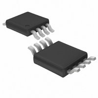
LTC1661CMS8 Linear Technology, LTC1661CMS8 Datasheet - Page 7

LTC1661CMS8
Manufacturer Part Number
LTC1661CMS8
Description
IC D/A CONV 10BIT MICRPWR 8-MSOP
Manufacturer
Linear Technology
Datasheet
1.LTC1661CMS8PBF.pdf
(14 pages)
Specifications of LTC1661CMS8
Settling Time
30µs
Number Of Bits
10
Data Interface
Serial
Number Of Converters
2
Voltage Supply Source
Single Supply
Power Dissipation (max)
260µW
Operating Temperature
0°C ~ 70°C
Mounting Type
Surface Mount
Package / Case
8-MSOP, Micro8™, 8-uMAX, 8-uSOP,
Lead Free Status / RoHS Status
Contains lead / RoHS non-compliant
Available stocks
Company
Part Number
Manufacturer
Quantity
Price
Company:
Part Number:
LTC1661CMS8
Manufacturer:
LINEAR
Quantity:
7
Part Number:
LTC1661CMS8
Manufacturer:
LINEAR/凌特
Quantity:
20 000
Company:
Part Number:
LTC1661CMS8#PBF
Manufacturer:
LT
Quantity:
7 920
Company:
Part Number:
LTC1661CMS8#TRPBF
Manufacturer:
LT
Quantity:
7 920
DEFINITIONS
Differential Nonlinearity (DNL): The difference between
the measured change and the ideal 1LSB change for any
two adjacent codes. The DNL error between any two codes
is calculated as follows:
where ∆V
two adjacent codes.
Full-Scale Error (FSE): The deviation of the actual full-scale
voltage from ideal. FSE includes the effects of offset and
gain errors (see Applications Information).
Integral Nonlinearity (INL): The deviation from a straight
line passing through the endpoints of the DAC transfer
curve (endpoint INL). Because the output cannot go
below zero, the linearity is measured between full scale
and the lowest code which guarantees the output will be
greater than zero. The INL error at a given input code is
calculated as follows:
where V
the given input code.
DNL =
INL =
OUT
V
OUT
∆V
OUT
is the output voltage of the DAC measured at
OUT
is the measured voltage difference between
LSB
– V
– LSB
OS
– V
(
LSB
FS
– V
OS
)
Code
1023
Least Significant Bit (LSB): The ideal voltage difference
between two successive codes.
Resolution (n): Defines the number of DAC output states
(2n) that divide the full-scale range. Resolution does not
imply linearity.
Voltage Offset Error (V
output when the DAC is loaded with all zeros. A single
supply DAC can have a true negative offset, but the out-
put cannot go below zero (see Applications Information).
For this reason, single supply DAC offset is measured at
the lowest code that guarantees the output will be greater
than zero.
LSB =
1024
V
REF
OS
): Nominally, the voltage at the
LTC1661
1661fa
7


