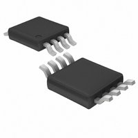
LTC1661CMS8 Linear Technology, LTC1661CMS8 Datasheet - Page 10

LTC1661CMS8
Manufacturer Part Number
LTC1661CMS8
Description
IC D/A CONV 10BIT MICRPWR 8-MSOP
Manufacturer
Linear Technology
Datasheet
1.LTC1661CMS8PBF.pdf
(14 pages)
Specifications of LTC1661CMS8
Settling Time
30µs
Number Of Bits
10
Data Interface
Serial
Number Of Converters
2
Voltage Supply Source
Single Supply
Power Dissipation (max)
260µW
Operating Temperature
0°C ~ 70°C
Mounting Type
Surface Mount
Package / Case
8-MSOP, Micro8™, 8-uMAX, 8-uSOP,
Lead Free Status / RoHS Status
Contains lead / RoHS non-compliant
Available stocks
Company
Part Number
Manufacturer
Quantity
Price
Company:
Part Number:
LTC1661CMS8
Manufacturer:
LINEAR
Quantity:
7
Part Number:
LTC1661CMS8
Manufacturer:
LINEAR/凌特
Quantity:
20 000
Company:
Part Number:
LTC1661CMS8#PBF
Manufacturer:
LT
Quantity:
7 920
Company:
Part Number:
LTC1661CMS8#TRPBF
Manufacturer:
LT
Quantity:
7 920
LTC1661
OPERATION
Voltage Outputs
Each of the rail-to-rail output amplifiers contained in the
LTC1661 can typically source or sink up to 5mA (V
The outputs swing to within a few millivolts of either supply
when unloaded and have an equivalent output resistance of
85Ω (typical) when driving a load to the rails. The output
amplifiers are stable driving capacitive loads up to 1000pF .
A small resistor placed in series with the output can be
used to achieve stability for any load capacitance. A 1µF
load can be successfully driven by inserting a 20Ω resis-
tor in series with the V
10Ω resistor, and a 10µF electrolytic capacitor can be used
without any resistor (the equivalent series resistance of the
capacitor itself provides the required small resistance). In
any of these cases, larger values of resistance, capacitance
or both may be substituted for the values given.
10
NEGATIVE
OFFSET
VOLTAGE
OUTPUT
Figure 2. Effects of Rail-to-Rail Operation On a DAC Transfer Curve. (2a) Overall Transfer Function (2b) Effect of Negative
Offset for Codes Near Zero Scale (2c) Effect of Positive Full-Scale Error for Input Codes Near Full Scale When V
0V
OUT
INPUT CODE
pin. A 2.2µF load needs only a
(2b)
VOLTAGE
OUTPUT
0
CC
= 5V).
INPUT CODE
V
REF
512
(2a)
= V
Rail-to-Rail Output Considerations
In any rail-to-rail DAC, the output swing is limited to volt-
ages within the supply range.
If the DAC offset is negative, the output for the lowest
codes limits at 0V as shown in Figure 2b.
Similarly, limiting can occur near full scale when the REF
pin is tied to V
error (FSE) is positive, the output for the highest codes
limits at V
can occur if V
Offset and linearity are defined and tested over the region
of the DAC transfer function where no output limiting can
occur.
CC
CC
1023
as shown in Figure 2c. No full-scale limiting
REF
CC
. If V
is less than V
REF
V
= V
REF
INPUT CODE
= V
(2c)
CC
CC
CC
and the DAC full-scale
– FSE.
REF
= V
CC
OUTPUT
VOLTAGE
POSITIVE
FSE
1661 F02
1661fa


