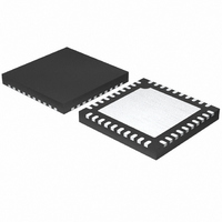
MAX5852ETL+ Maxim Integrated Products, MAX5852ETL+ Datasheet - Page 13

MAX5852ETL+
Manufacturer Part Number
MAX5852ETL+
Description
IC DAC 8BIT DUAL 165MSPS 40-TQFN
Manufacturer
Maxim Integrated Products
Datasheet
1.MAX5852ETL.pdf
(18 pages)
Specifications of MAX5852ETL+
Settling Time
12ns
Number Of Bits
8
Data Interface
Parallel
Number Of Converters
2
Voltage Supply Source
Single Supply
Operating Temperature
-40°C ~ 85°C
Mounting Type
Surface Mount
Package / Case
40-TQFN Exposed Pad
Lead Free Status / RoHS Status
Lead free / RoHS Compliant
Power Dissipation (max)
-
The CLK pin now becomes an output, and provides a
single-ended replica of the differential clock signal,
which may be used to synchronize the input data. Data is
written to the device on the rising edge of the CLK signal.
The MAX5852 provides an integrated 50ppm/°C, 1.24V,
low-noise bandgap reference that can be disabled and
overridden with an external reference voltage. REFO
serves either as an external reference input or an inte-
grated reference output. If REN =0, the internal refer-
ence is selected and REFO provides a 1.24V (50µA)
output. Buffer REFO with an external amplifier, when
driving a heavy load.
The MAX5852 also employs a control amplifier
designed to simultaneously regulate the full-scale out-
put current (I
Calculate the output current as:
where I
V
R
amplifier output current of the MAX5852 (Figure 3). This
current is mirrored into the current-source array where
I
ments and summed to valid output current readings for
the DACs.
Figure 3. Setting I
Control Amplifier
FS
REFO
SET
*COMPENSATION CAPACITOR (C
Internal Reference and Control Amplifier
is equally distributed between matched current seg-
AGND
OPTIONAL EXTERNAL BUFFER
FOR HEAVIER LOADS
is the reference resistor that determines the
I
/ R
MAX4040
REF
REF
=
SET
V
R
REF
SET
is the reference output current (I
) and I
FS
Dual, 8-Bit, 165Msps, Current-Output DAC
FS
AGND
) for both outputs of the devices.
with the Internal 1.24V Reference and the
C
______________________________________________________________________________________
COMP
COMP
I
FS
FS
*
REFO
REFR
R
SET
≈ 100nF)
= 32
is the full-scale output current.
I
REF
REFERENCE
BANDGAP
1.24V
I
REF
MAX5852
REN = 0
CURRENT-
SOURCE
ARRAY
REF
I
FS
=
To disable the internal reference of the MAX5852, set
REN = 1. Apply a temperature-stable, external reference
to drive the REFO pin and set the full-scale output
(Figure 4). For improved accuracy and drift perfor-
mance, choose a fixed-output voltage reference such as
the 1.2V, 25ppm/°C MAX6520 bandgap reference.
The MAX5852 accepts an input data and the DAC con-
version rate of up to 165Msps. The input latches on the
rising edge of the clock, whereas the output latches on
the following rising edge.
Figure 5 depicts the write cycle of the two DACs in non-
interleaved mode.
The MAX5852 can also operate in an interleaved data
mode. Programming the IDE bit with a high level activates
this mode (Tables 1 and 2). In interleaved mode, data for
both DAC channels is written through input port A.
Channel B data is written on the falling edge of the clock
signal and then channel A data is written on the following
rising edge of the clock signal. Both DAC outputs (chan-
nel A and B) are updated simultaneously on the next fol-
lowing rising edge of the clock. In interleaved data mode,
the maximum input data rate per channel is half of the
rate in noninterleaved mode. The interleaved data mode
is attractive for applications where lower data rates are
acceptable and interfacing on a single 8-bit bus is
desired (Figure 6).
Figure 4. MAX5852 with External Reference
MAX6520
REFERENCE
EXTERNAL
AGND
1.2V
AV
DD
AGND
REFO
REFR
R
SET
I
REF
REFERENCE
BANDGAP
1.24V
External Reference
AV
MAX5852
DD
10µF
Detailed Timing
REN = 1
AGND
CURRENT-
SOURCE
ARRAY
0.1µF
I
FS
13


