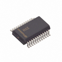
MAX5190BEEG+ Maxim Integrated Products, MAX5190BEEG+ Datasheet - Page 8

MAX5190BEEG+
Manufacturer Part Number
MAX5190BEEG+
Description
IC DAC 8BIT 40MHZ VOUT 24-QSOP
Manufacturer
Maxim Integrated Products
Datasheet
1.MAX5190BEEG.pdf
(15 pages)
Specifications of MAX5190BEEG+
Settling Time
25µs
Number Of Bits
8
Data Interface
Parallel
Number Of Converters
1
Voltage Supply Source
Analog and Digital
Operating Temperature
-40°C ~ 85°C
Mounting Type
Surface Mount
Package / Case
24-QSOP
Number Of Dac Outputs
1
Resolution
8 bit
Interface Type
Parallel
Supply Voltage (max)
3.3 V
Supply Voltage (min)
2.7 V
Maximum Operating Temperature
+ 85 C
Mounting Style
SMD/SMT
Maximum Power Dissipation
762 mW
Minimum Operating Temperature
- 40 C
Supply Current
4.2 mA
Lead Free Status / RoHS Status
Lead free / RoHS Compliant
Power Dissipation (max)
-
Lead Free Status / Rohs Status
Lead free / RoHS Compliant
8-Bit, 40MHz, Current/Voltage-Output DACs
Figure 1. Functional Diagram
The MAX5187/MAX5190 are 8-bit DACs capable of
operating with clock speeds up to 40MHz. Each con-
verter consists of separate input and DAC registers, fol-
lowed by a current-source array capable of generating
up to 1.5mA full-scale output current (Figure 1). An inte-
grated +1.2V voltage reference and control amplifier
determine the data converters’ full-scale output cur-
rents/voltages. Careful reference design ensures close
gain matching and excellent drift characteristics. The
MAX5190’s voltage-output operation features matched
400Ω on-chip resistors that convert the current array
current into a voltage.
The MAX5187/MAX5190 provide an integrated
50ppm/°C, +1.2V, low-noise bandgap reference that
can be disabled and overridden by an external refer-
ence voltage. REFO serves either as an external refer-
ence input or an integrated reference output. If REN is
connected to DGND, the internal reference is selected
and REFO provides a +1.2V output. Due to its limited
8
_______________________________________________________________________________________
*INTERNAL 400Ω AND 9.6kΩ
Detailed Description
CLK
REFO
REFR
RESISTORS FOR MAX5190 ONLY.
and Control Amplifier
9.6k*
Internal Reference
1.2V REF
REN
MSB DECODE
LATCHES
LATCHES
OUTPUT
INPUT
AV
DAC SWITCHES
DD
D7–D0
SOURCE ARRAY
CURRENT-
AGND
MSB DECODE
LATCHES
LATCHES
OUTPUT
INPUT
10µA output drive capability, REFO must be buffered
with an external amplifier if heavier loading is required.
The MAX5187/MAX5190 also employ a control amplifi-
er, designed to simultaneously regulate the full-scale
output current (I
output current is calculated as follows:
where I
V
R
amplifier’s output current on the MAX5187 (Figure 2).
This current is mirrored into the current-source array,
where it is equally distributed between matched current
segments and summed to valid output current readings
for the DACs.
The MAX5190 converts this output current into a differ-
ential output voltage (V
referenced 400Ω load resistors. Using the internal
+1.2V reference voltage, the MAX5190’s integrated
reference output current resistor (R
I
REF
REFO /
SET
to 125µA and I
CS
is the reference resistor that determines the
REF
R
SET
DACEN
is the reference output current (I
) and I
400Ω
DV
MAX5187
MAX5190
DD
FS
*
) for both outputs of the devices. The
FS
PD
DGND
FS
I
FS
400Ω*
to 1mA.
OUT
is the full-scale output current.
= 8 x I
) with two internal, ground-
OUTP
OUTN
CREF
REF
SET
= 9.6kΩ) sets
REF
=


