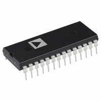
AD569JNZ Analog Devices Inc, AD569JNZ Datasheet - Page 2

AD569JNZ
Manufacturer Part Number
AD569JNZ
Description
IC DAC 16BIT MONO 28-DIP
Manufacturer
Analog Devices Inc
Datasheet
1.AD569JNZ.pdf
(12 pages)
Specifications of AD569JNZ
Data Interface
Parallel
Settling Time
4µs
Number Of Bits
16
Number Of Converters
1
Voltage Supply Source
Dual ±
Operating Temperature
0°C ~ 70°C
Mounting Type
Through Hole
Package / Case
28-DIP (0.600", 15.24mm)
Resolution (bits)
16bit
Input Channel Type
Parallel
Supply Current
9mA
Digital Ic Case Style
DIP
No. Of Pins
28
Operating Temperature Range
0°C To +70°C
Supply Voltage Range - Analog
± 10.8V To ± 13.2V
Rohs Compliant
Yes
Lead Free Status / RoHS Status
Lead free / RoHS Compliant
Power Dissipation (max)
-
Lead Free Status / RoHS Status
Lead free / RoHS Compliant, Lead free / RoHS Compliant
AD569–SPECIFICATIONS
Model
Parameter
RESOLUTION
TRANSFER FUNCTION
REFERENCE INPUT
OUTPUT CHARACTERISTICS
POWER SUPPLIES
TEMPERATURE RANGE
NOTES
1
2
3
4
5
Specifications subject to change without notice.
Specifications shown in boldface are tested on all production units at final electrical test. Results from those tests are used to calculate outgoing quality levels. All min
and max specifications are guaranteed, although only those shown in boldface are tested on all production units.
FSR stands for Full-Scale Range, and is 10 V for a –5 V to +5 V span.
Refer to Definitions section.
For operation with supplies other than 12 V, refer to the Power Supply and Reference Voltage Range Section.
Measured between +V
Sensitivity of Full-Scale Error due to changes in +V
LOGIC INPUTS
CHARACTERISTICS
+V
–V
Resistance
Voltage
Capacitive Load
Resistive Load
Short Circuit Current
Voltage
Current
Power Supply Sensitivity
Specified
Storage
V
V
I
I
Integral Nonlinearity
Differential Nonlinearity
Unipolar Offset
Bipolar Offset
Full Scale Error
Bipolar Zero
+V
–V
+I
–I
+10.8 V
–10.8 V
JN, KN, JP, KP
AD, BD
SD
JN, KN, JP, KP
AD, BD, SD
IH
IL
REF
REF
IH
IL
T
T
T
T
T
T
S
S
S
(V
S
(V
(Logic “l”)
MIN
MIN
MIN
MIN
MIN
MIN
(Logic “0”)
Range
Range
IL
IH
to T
to T
to T
to T
to T
to T
= 0 V)
= 5.5 V)
–V
+V
3
MAX
MAX
MAX
MAX
MAX
MAX
2
S
2
S
2
2
–13.2 V
+13.2 V
REF
Force and –V
5
REF
Min
2.0
0
–5
–5
15
–5
1
+10.8
–10.8
0
–25
–65
–65
Force.
AD569JN/JP/AD
S
and sensitivity of Offset to changes in –V
Typ
20
10
+12
–12
+9
–9
0.02
0.02
1/2
1/2
0.5
1
(T
otherwise noted.)
A
= +25 C, +V
Max
16
5.5
0.8
10
10
+5
+5
25
+5
1000
+13.2
–13.2
+13
–13
+70
+85
+150
+150
0.04
0.04
1
1
500
750
500
750
350
750
0.04
0.04
2
3
Min
2.0
0
–5
–5
15
–5
1
+10.8
–10.8
0
–25
–65
–65
–2–
S
AD569KN/KP/BD
= +12 V, –V
Typ
20
10
+12
–12
+9
–9
0.01
0.020
1/4
1/2
0.5
1
S
.
S
= –12 V, +V
Max
16
5.5
0.8
10
10
+5
+5
25
+5
1000
+13.2
–13.2
+13
–13
+70
+85
+150
+150
0.024
0.024
1/2
1
350
450
350
450
350
750
0.024
0.024
2
3
REF
= +5 V, –V
Min
2.0
0
–5
–5
15
–5
1
+10.8
–10.8
–55
–65
AD569SD
Typ
20
10
+12
–12
+9
–9
REF
0.5
1
= –5 V, unless
Max
16
5.5
0.8
10
10
+5
+5
25
+5
1000
+13.2
–13.2
+13
–13
+125
+150
0.04
0.04
1
1
500
750
500
750
350
750
0.04
0.04
2
3
Units
mA
Bits
Volts
Volts
% FSR
% FSR
LSB
LSB
% FSR
% FSR
Volts
Volts
k
Volts
pF
k
Volts
Volts
mA
mA
ppm/%
ppm/%
C
C
C
C
C
A
A
V
V
V
V
V
V
REV. A
4
1


