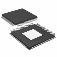
AD9785BSVZ Analog Devices Inc, AD9785BSVZ Datasheet - Page 25

AD9785BSVZ
Manufacturer Part Number
AD9785BSVZ
Description
IC DAC 12BIT 800MSPS 100TQFP
Manufacturer
Analog Devices Inc
Series
TxDAC®r
Datasheet
1.AD9785BSVZ.pdf
(64 pages)
Specifications of AD9785BSVZ
Data Interface
Serial
Number Of Bits
12
Number Of Converters
2
Voltage Supply Source
Analog and Digital
Power Dissipation (max)
450mW
Operating Temperature
-40°C ~ 85°C
Mounting Type
Surface Mount
Package / Case
100-TQFP Exposed Pad, 100-eTQFP, 100-HTQFP, 100-VQFP
Resolution (bits)
12bit
Sampling Rate
800MSPS
Input Channel Type
Parallel
Digital Ic Case Style
QFP
No. Of Pins
100
Operating Temperature Range
-40°C To +85°C
Lead Free Status / RoHS Status
Lead free / RoHS Compliant
Settling Time
-
Lead Free Status / RoHS Status
Lead free / RoHS Compliant, Lead free / RoHS Compliant
Available stocks
Company
Part Number
Manufacturer
Quantity
Price
Company:
Part Number:
AD9785BSVZ
Manufacturer:
Analog Devices Inc
Quantity:
135
Company:
Part Number:
AD9785BSVZ
Manufacturer:
Analog Devices Inc
Quantity:
10 000
Company:
Part Number:
AD9785BSVZRL
Manufacturer:
Analog Devices Inc
Quantity:
10 000
Address
0x0B
0x0C
0x0D
0x0E
0x1D
0x1E
1
SPI REGISTER DESCRIPTIONS
The communication (COMM) register comprises one byte located at Address 0x00.
Table 10. Communication (COMM) Register
Address
0x00
Address space between Address 0x0E and Address 0x1D is intentionally left open.
1
1
Register
Name
Phase
Control
Register
Amplitude
Scale
Factor
Register
Output
Offset
Register
Version
Register
RAM
Test
Register
Bit
[7]
[6]
[5]
[4]
[3]
[2]
[1]
SPI_SDIO
bidirectional
LSB first
Software reset
Power-down mode
Auto power-down
enable
I/O transfer
(self-reset)
Automatic I/O
transfer enable
Name
Bit
Range
[15:0]
[23:16]
[31:24]
[7:0]
[15:8]
[23:16]
[15:0]
[31:16]
[7:0]
[15:8]
[31:0]
[23:0]
MSB
Description
0: Default. Use the SPI_SDIO pin for input data only, 4-wire serial mode.
1: Use SPI_SDIO as a read/write pin, 3-wire serial mode.
0: Default. MSB first format is active.
1: Serial interface accepts serial data in LSB first format.
0: Default. Bit is in the inactive state.
1: In the AD9785/AD9787/AD9788, all programmable bits return to their power-up state
except for the COMM register bits, which are unaffected by the software reset. The software
reset remains in effect until this bit is set to 0 (inactive state).
0: Default. The full chip power-down is not active.
1: The AD9785/AD9787/AD9788 enter a power-down mode in which all functions are
powered down. This power-down puts the part into its lowest possible power dissipation
state. The part remains in this low power state until the user sets this bit to a Logic 0. The
analog circuitry requires 250 ms to become operational.
0: Default. Inactive state, automatic power-down feature is not enabled.
1: The device automatically switches into its low power mode whenever TXENABLE is
deasserted for a sufficiently long period of time.
0: Default. Inactive state.
1: The contents of the frequency tuning word memory buffer, phase control memory buffer,
amplitude scale factor memory buffer, and the output offset memory buffer are moved to a
memory location that affects operation of the device. The one-word memory buffer is
employed to simultaneously update the NCO frequency, phase, amplitude, and offset control.
Note that this bit automatically clears itself after the I/O transfer occurs. For this reason,
unless the reference clock is stopped, it is difficult to read back a Logic 1 on this bit.
0: Automatic I/O transfer disabled. The I/O transfer bit (Bit 2) must be set to update the device
in the event that changes have been made to Register 0x0A, Register 0x0B, Register 0x0C, or
Register 0x0D. This allows the user to change important operating modes of the device all at
once, rather than one at a time with individual SPI writes.
1: Default. Automatic I/O transfer enabled. The device updates its operation immediately
when SPI writes are completed to Register 0x0A, Register 0x0B, Register 0x0C, or Register 0x0D.
MSB − 1
Q DAC Amplitude Scale Factor [6:0]
Rev. A | Page 25 of 64
MSB − 2
Reserved
Reserved
I DAC Amplitude Scale Factor [7:0]
NCO Phase Offset Word [15:0]
Phase Correction Word [7:0]
Q DAC Offset [15:0]
I DAC Offset [15:0]
MSB − 3
Version ID
Reserved
RAM
Test
MSB − 4
MSB − 5
AD9785/AD9787/AD9788
MSB − 6
Q DAC Amplitude Scale
Phase Correction Word
Factor [8:7]
[9:8]
LSB
I DAC
Amplitude
Scale
Factor [8]
Default
0x00
0x00
0x00
0x80
0x00
0x01
0x00
0x00


