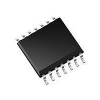
MCP4912-E/ST Microchip Technology, MCP4912-E/ST Datasheet - Page 19

MCP4912-E/ST
Manufacturer Part Number
MCP4912-E/ST
Description
DAC 10BIT DUAL W/SPI 14TSSOP
Manufacturer
Microchip Technology
Datasheet
1.MCP4922-EP.pdf
(48 pages)
Specifications of MCP4912-E/ST
Number Of Converters
2
Settling Time
4.5µs
Package / Case
14-TSSOP
Number Of Bits
10
Data Interface
Serial, SPI™
Voltage Supply Source
Single Supply
Operating Temperature
-40°C ~ 125°C
Mounting Type
Surface Mount
Number Of Dac Outputs
2
Resolution
10 bit
Interface Type
SPI
Supply Voltage (max)
6.5 V
Supply Voltage (min)
2.7 V
Maximum Operating Temperature
+ 125 C
Mounting Style
SMD/SMT
Minimum Operating Temperature
- 55 C
Supply Current
350 uA
Lead Free Status / RoHS Status
Lead free / RoHS Compliant
Power Dissipation (max)
-
Lead Free Status / Rohs Status
Lead free / RoHS Compliant
Available stocks
Company
Part Number
Manufacturer
Quantity
Price
Company:
Part Number:
MCP4912-E/ST
Manufacturer:
MICROCHIP
Quantity:
12 000
Part Number:
MCP4912-E/ST
Manufacturer:
MICROCHIP/微芯
Quantity:
20 000
4.0
The MCP4902, MCP4912 and MCP4922 are dual
voltage-output 8-bit, 10-bit and 12-bit DAC devices,
respectively. These devices include input amplifiers,
rail-to-rail output amplifiers, reference buffers for
external
reset-management circuitry. The devices use an SPI
serial communication interface and operate with a
single supply voltage from 2.7V to 5.5V.
The DAC input coding of these devices is straight
binary.
voltage calculation.
EQUATION 4-1:
The ideal output range of each device is:
• MCP4902 (n = 8)
(a) 0 V to 255/256 * V
(b) 0 V to 255/256 * 2 * V
• MCP4912 (n = 10)
(a) 0 V to 1023/1024 * V
(b) 0 V to 1023/1024 * 2 * V
• MCP4922 (n = 12)
(a) 0 V to 4095/4096 * V
(b) 0 V to 4095/4096 * 2 * V
1 LSb is the ideal voltage difference between two
successive codes.
calculation of each device.
2010 Microchip Technology Inc.
Where:
V
Note:
REF
D
G
n
n
Equation 4-1
GENERAL OVERVIEW
=
=
=
=
=
=
=
=
=
V
See the output swing voltage specification
in Section 1.0 “Electrical Characteris-
tics”.
voltage
OUT
E
2 for <GA> bit = 0
1 for <GA> bit = 1
DAC Resolution
8 for MCP4902
10 for MCP4912
12 for MCP4922
DAC input code
Gain Selection
X
ternal voltage reference
=
------------------------------ - G
V
REF
shows the DAC analog output
Table 4-1
ANALOG OUTPUT
VOLTAGE (V
REF
reference,
REF
REF
2
REF
when gain setting = 1x.
n
REF
REF
when gain setting = 1x.
when Gain setting = 1x.
D
when gain setting = 2x.
n
when gain setting = 2x.
when gain setting = 2x.
illustrates the LSb
shutdown
OUT
)
and
TABLE 4-1:
4.1
4.1.1
Integral Non-Linearity (INL) error is the maximum
deviation between an actual code transition point and
its corresponding ideal transition point, after offset and
gain errors have been removed. The two end points
(from 0x000 and 0xFFF) method is used for the calcu-
lation.
A positive INL error represents transition(s) later than
ideal. A negative INL error represents transition(s) ear-
lier than ideal.
FIGURE 4-1:
4.1.2
A Differential Non-Linearity (DNL) error is the measure
of variations in code widths from the ideal code width.
A DNL error of zero indicates that every code is exactly
1 LSb wide.
where V
MCP4902/4912/4922
Digital
Input
Code
MCP4902
MCP4912
MCP4922
(n = 10)
(n = 12)
Device
(n = 8)
Figure 4-1
REF
DC Accuracy
INL ACCURACY
DNL ACCURACY
111
110
101
100
011
010
001
000
is the external voltage reference.
Selection
shows the details.
LSb OF EACH DEVICE
Gain
Actual
Transfer
Function
1x
2x
1x
2x
1x
2x
Example for INL Error.
DAC Output
V
(2* V
V
(2* V
V
(2* V
REF
REF
REF
INL < 0
INL < 0
/256
/1024
/4096
REF
REF
REF
LSb Size
DS22250A-page 19
)/256
)/1024
)/4096
Ideal Transfer
Function


