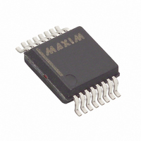
MAX5312EAE+ Maxim Integrated Products, MAX5312EAE+ Datasheet - Page 14

MAX5312EAE+
Manufacturer Part Number
MAX5312EAE+
Description
IC DAC 12BIT 5V/10V SER 16-SSOP
Manufacturer
Maxim Integrated Products
Datasheet
1.MAX5312EAE.pdf
(19 pages)
Specifications of MAX5312EAE+
Settling Time
10µs
Number Of Bits
12
Data Interface
Serial
Number Of Converters
1
Voltage Supply Source
Dual ±
Operating Temperature
-40°C ~ 85°C
Mounting Type
Surface Mount
Package / Case
16-SSOP
Number Of Dac Outputs
1
Resolution
12 bit
Interface Type
Serial (SPI)
Supply Voltage (max)
15.75 V
Supply Voltage (min)
10.8 V
Maximum Operating Temperature
+ 85 C
Mounting Style
SMD/SMT
Maximum Power Dissipation
571 mW
Minimum Operating Temperature
- 40 C
Supply Current
30 uA
Voltage Reference
External
Lead Free Status / RoHS Status
Lead free / RoHS Compliant
Power Dissipation (max)
-
Lead Free Status / Rohs Status
Lead free / RoHS Compliant
Data in the shift register is transferred to the input register
during the appropriate software command only. Data in
the input register is transferred to the DAC register in one
of two ways: using the software command, or through
external logic control using the asynchronous load input
(LDAC).
transfer the data from the shift register to the input and/or
DAC registers. The CLR, an external logic control, asyn-
chronously forces the input and DAC registers to zero
code, and the output to 0V, in both unipolar and bipolar
modes. The interface timing is shown in Figures 2 and 3.
Wait a minimum of 100ns after CS goes high before
implementing LDAC or CLR. If either of these logic
inputs activates during a data transfer, the incoming
data is corrupted and needs to be reloaded. For soft-
ware control only, connect LDAC and CLR high.
±10V, 12-Bit, Serial, Voltage-Output DAC
Table 1. Serial-Data Format
Table 2. Serial-Interface Programming Commands
X = Don’t care.
*All unlisted commands are reserved commands. Do not use.
Figure 2. Serial-Interface Signals
14
MSB
C3
C3
0
0
0
0
1
1
CONTROL BITS*
______________________________________________________________________________________
CONTROL BITS
C2
0
0
1
1
0
1
Table 2 shows the software commands that
SCLK
C2
DIN
CS
C1
0
1
0
1
0
0
C1
C3
C0
1
0
0
0
0
0
0
C2
C0
XXXXXXXXXXXX No operation; command is ignored.
12-bit DAC data
12-bit DAC data
XXXXXXXXXXXX Load D AC r eg i ster fr om i np ut r eg i ster ; D AC outp ut up d ated ; i np ut r eg i ster unchang ed .
XXXXXXXXXXXX Enter shutdown; input and DAC registers unchanged.
XXXXXXXXXXXX Exit shutdown; input and DAC registers unchanged.
INPUT DATA
C1
D11–D0
D11
C0
D11
D10
D10
Load input register from shift register; DAC output unchanged.
Load input and DAC registers from shift register; DAC output updated.
D9
D9
D8
8
D8
D7
9
The MAX5312 uses an inverted DAC ladder architec-
ture to convert the digital input into an analog output
voltage. The digital input controls weighted-switches
that connect the DAC ladder nodes to either REF or
GND (Figure 4). The sum of the weights produces the
analog equivalent of the digital-input word and is then
buffered at the output.
D7
D6
DATA BITS
D5
D6
D4
FUNCTION
D5
D3
COMMAND EXECUTED
D2
D4
D1
D3
D0
16
DAC Architecture
D2
(1)
D1
LSB
D0


